 180
180
AMD Ryzen Memory Tweaking & Overclocking Guide
(180 Comments) »Introduction
Update History:
- Apr 4th 2019: Completely rewrote and simplified the "Relations Between Memory Timings" page
My name is Yuri Bubly (@1usmus). I am the developer of the DRAM Calculator for Ryzen, author of numerous BIOS mods, and curator of dozens of topics about and related to these processors. After two years of research and development, I am ready to share my secrets on optimizing memory on a Ryzen-powered system. By optimization, I specifically mean overclocking and tuning of system RAM the right way—the way that won't break it.
You've probably pegged your "AMD vs. Intel" CPU choice on the complexity of memory overclocking on AMD Ryzen systems. I'm here to tell you that it is much easier than you think or were led to believe. The purpose of this guide is to show you what to look for when buying memory and how to quickly and correctly set up your system by avoiding common mistakes, and to show what results can be obtained by properly overclocking the RAM.

Some may ask what real benefits can be gained by memory overclocking. Well, for starters, my research shows gains of up to +50% FPS in games over the default values. Sounds tempting, doesn't it? You see, Ryzen processors are more sensitive to memory clock speeds than Intel processors. Ryzen processors synchronize the Infinity Fabric clock-speed to scale linearly with the memory clock. This is important since Infinity Fabric is the primary interconnect for all components on a "Zen" processor silicon, including the all-important link between two CCX (Zen compute complexes).
Due to the huge number of variables and nuances to be covered, the material will be divided into two parts: (1) theory, which contains a description of all the details relevant to memory settings and testing, and (2) results, which will demonstrate the impact optimized results have on games.
Glossary of Terms
Below is a list of technical terms relevant to overclocking the memory of a Ryzen-powered machine. Ryzen uses the industry-standard DDR4 memory architecture, so you may be familiar with some of these terms. Some other terms are new and specific to the "Zen" architecture.- SOC voltage - system on a chip voltage; responsible for the voltage related to the memory controller.
Limit: up to 1.2 V. - DRAM boot voltage - voltage at which memory training takes place at system start-up.
Limit: up to 1.45–1.50 V. - VDDP voltage - voltage for the transistor that sets memory contents.
Limit: up to 1.1 V. - CLDO VDDP voltage - voltage for the DDR4 PHY on the SoC. The DDR4 PHY or physical-layer interface converts information from the memory controllers to a format the DDR4 memory modules can understand.
Somewhat counterintuitively, lowering VDDP can often be more beneficial for stability than raising CLDO_VDDP. Advanced overclockers should also know that altering CLDO VDDP can move or resolve memory holes. Small changes to VDDP can have a big effect, and VDDP cannot not be set to a value greater than VDIMM - 0.1 V (not to exceed 1.05 V). A cold reboot is required if you alter this voltage.
Limit: up to 1.0 V. - VPP (VPPM) voltage - voltage that determines how reliably a DRAM row gets accessed.
Limit: up to 2.7 V. - Vref voltage - memory reference voltage; "Configures" both the CPU and the memory module with the voltage level that separates what is to be considered a "0" or a "1"; i.e., voltages found on the memory bus below MEMVREF are to be considered a "0," and voltages above this level are to be considered a "1." By default, this voltage level is half of VDDIO (a.k.a. 0.500x). Some motherboards allow the user to change this ratio, usually through two options: (1) "DRAM Ctrl Ref Voltage" (for the control lines from the memory bus; JEDEC's official name for this voltage is VREFCA), and (2) "DRAM Ctrl Data Ref Voltage" (for the data lines from the memory bus; JEDEC's official name is "VREFDQ"). These options are configured as a multiplier.
- VTT DDR voltage - voltage used to control the impedance of the bus in order to achieve the high speed and maintain signal integrity. This is done by resistor parallel termination.
- PLL (1P8) voltage - This option can be used to stabilize the CPU at high BCLKs.
Limit: up to 1.9 V. - CAD_BUS - Command & Address bus; for those who are able to train the memory at high speeds (>=3466MHz), but are unable to stabilize it due to signaling issues. I suggest you try decreasing "Command & Address" related drive currents (increasing the resistance).
Limit: None. - CAD_BUS timings - transceiver delay. Values set a bit mask.
Limit: None. - procODT - resistance value, in ohms, that determines how a completed memory signal is terminated. Higher values can help stabilize higher data rates.
Limit: None. - RTT (Signal Integrity Optimizations) - the use of multiple ranks of DRAM on the DDR4 interface requires additional options for selecting the on-die terminating resistance for individual ranks.
DDR4 DRAM offers a range of terminating resistance values. The specific DQ pin receiver resistance presented to the interface is selected by a combination of the initial chip configuration and the DRAM operating command if dynamic on-die termination is enabled.
Limit: None. - Geardown Mode - allows the DRAM device to run off its internally-generated ½ rate clock for latching on the command or address buses.
ON is the default for speeds greater than DDR4-2667. However, the benefit of ON vs. OFF will vary from memory kit to memory kit. Enabling Geardown Mode will override your current command rate. - Power Down Mode - can modestly save system power at the expense of higher DRAM latency by putting DRAM into a quiescent state after a period of inactivity.
Theory: Infinity Fabric and Types of RAM
As we mentioned earlier, Infinity Fabric is the all-important interconnect AMD deployed to link the various on-die components on "Zen" processors, including the CPU compute complexes (groups of up to 4 CPU cores). Infinity Fabric has its own clock domain, although that clock is synchronized with the memory clock speed.Structurally, Infinity Fabric is a 256-bit bidirectional bus. With its help, in the six-core and eight-core models of Ryzen processors, two quad-core complexes (CCX) exchange data with other blocks, including the root PCIe complex and the south bridge. The frequency of Infinity Fabric has been designed to match the frequency of system RAM. For example, if the memory controller works at DDR4-2133, the matrix of the switch synchronizes at a frequency of 1066 MHz (recall, the effective frequency is indicated in the memory designation). This means that faster memory allows you to increase the bandwidth of the internal Infinity Fabric connection.
This technology introduces great prospects when creating multi-core processors. I also want to note that a newer version of this bus will be implemented in new Zen 2 processors, which are multi-chip modules of up to three dies on the AM4 package—up to two CPU dies and an I/O controller die.
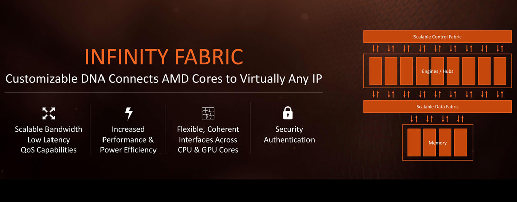
Looking at the picture, you can see that the bottleneck in this situation is RAM. We need high frequency and low latency for faster data access.
Memory Types
Over the past decade, Intel has sown the idea in people's heads that RAM is a decorative component. Sometimes, it has decorative LED lighting or stylish heatsinks to look cool. By the way of the general idea that RAM is more about style, people stopped thinking about its real significance.At the moment, there are a huge number of options on the RAM market that may interest us, with tons of features trying to differentiate them from their competitors. Some of these features are wonderful, but some may be completely useless for some users. How does one choose what is best for them?
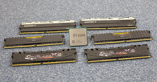
One of the best memory for overclocking—probably the best based on my testing—is Samsung b-die (20 nm) RAM, often coming with record frequency and latency out of the box. I want to make an important point here—you don't have to buy an expensive kit with impressive-looking high frequencies of 4200+ MHz in order to achieve the performance you are looking for. In most cases, overclocking such a kit will be comparable to that of a 3000 MHz kit with a CAS latency ("CL") of 14. Of course, the silicon lottery is always a factor, and it may turn out that a 3000 MHz kit at CL14 can outperform a 3600 MHz kit that just won't run stable. I will demonstrate this later in this article with some of the memory I reviewed.
The first on the list for examination is the G.Skill Sniper X 3400C16. This is a single-rank DIMM with unremarkable stock settings and timings, at least in contrast to the results obtained after overclocking.

The above screenshot shows that time spent overclocking memory is worth it. I was able to achieve a speed of 3667 MHz at CL14. In other testing, I also managed to achieve the cherished 3733 MHz at CL14 on these modules, but not without using a rather high voltage of 1.51 V. 1.51 V is in my opinion not suitable for everyday use as there is a chance of degradation and premature death of the memory modules.

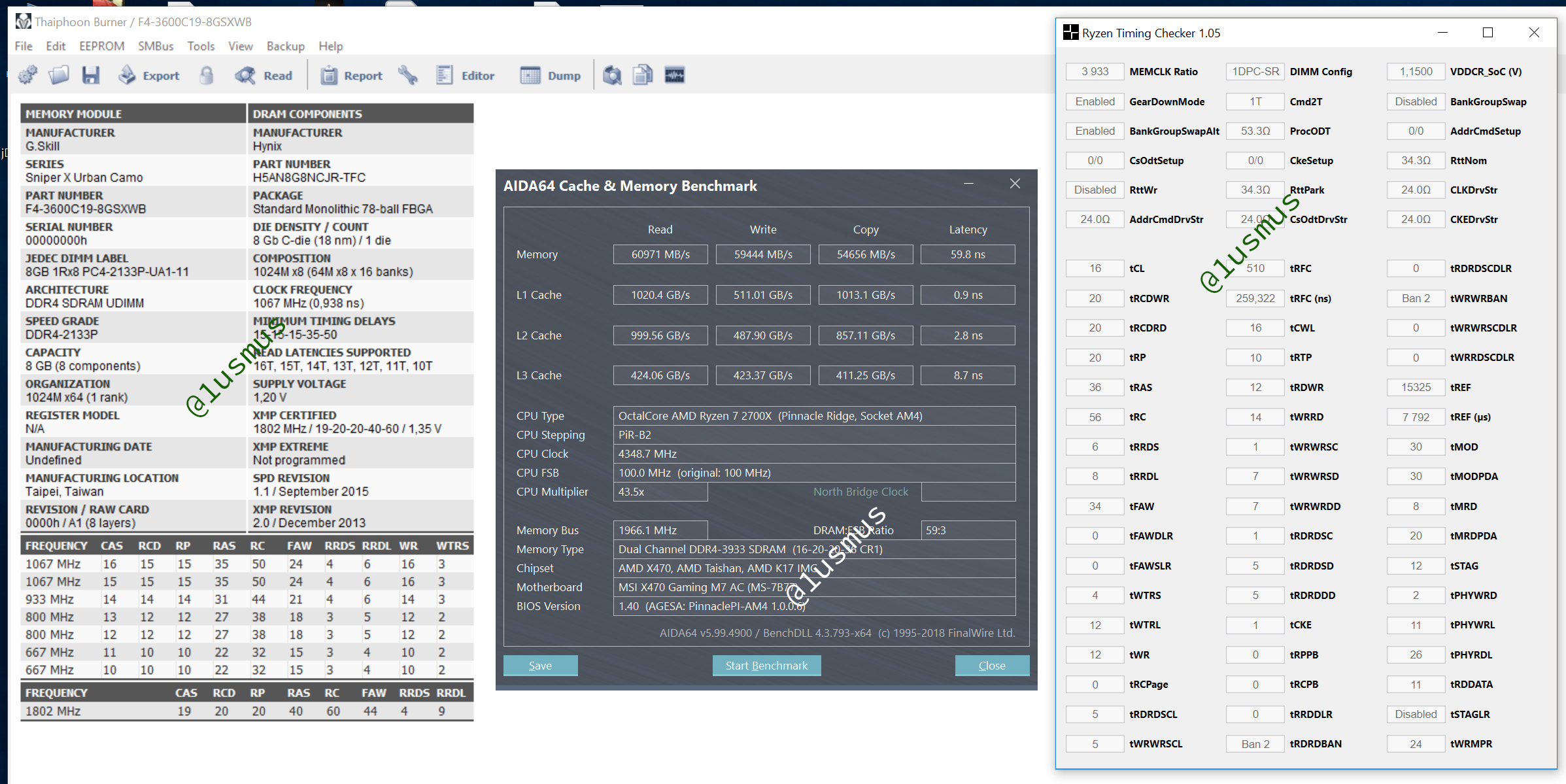
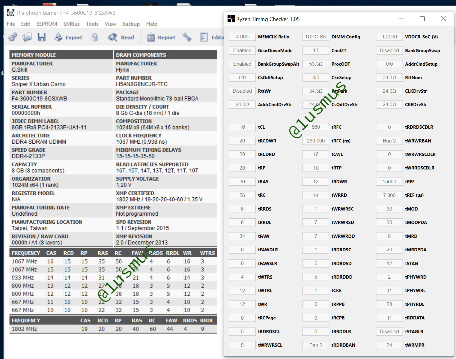
Next on my list of recommended memory are modules based on SK-Hynix CJR chips (18 nm). To illustrate this, I used a set of G.Skill Sniper X 3600 C19 modules. This memory kit is almost half the price of the Samsung b-die based Sniper X 3400 memory and lacks the "AMD Ryzen compatible" sticker. Thinking that like Flare X, the Sniper X series is "Ryzen-friendly" across the board, many uninformed Ryzen buyers could be drawn to this kit.
With this kit, I was able to achieve 3933 MHz at CL16, the absolute frequency record in my findings for frequency and throughput. I had to trade some CAS latency for that speed, though.
And this is not the limit! Stepping it up further to 4000 CL16 is realistic.
Because of this, the latest version of my calculator includes presets of up to 3867 MHz for memory kits with SK-Hynix CJR memory modules.
This year also saw the introduction of new Micron H/E-die (16 nm) memory modules. Unfortunately, I have not yet been able to get my hands on these chips. According to some preliminary testing by my colleagues, the memory is similarly good at overclocking, making kits with these memory modules worthy contender for consideration.
And what about dual-rank DIMMs? By comparison, results of overclocking dual-rank RAM configurations are pretty sad at the moment. The memory controller has difficulty handling four ranks right now. I was able to achieve 3400 MHz CL14 with Samsung b-die memory modules and 3600 MHz CL16 with Hynix CJR memory modules. Based on my testing, the only upside to using four ranks is the impressive capacity increase and alternation because of the ranks technology, which increases system performance in games.
3600 MHz CL16 is still a big gain considering AMD's documentation states that Ryzen processors are limited to 2400 MHz when using two dual-rank modules. So far, going dual-rank has been the only way memory manufacturers have been able to build client-segment 16 GB modules (making up 32 GB dual-channel kits). If you really need over 16 GB of RAM, you must trim your overclocking expectations accordingly.
Our Patreon Silver Supporters can read articles in single-page format.
May 1st, 2024 16:34 EDT
change timezone
Latest GPU Drivers
New Forum Posts
- Alphacool CORE 1 CPU block - bulging with danger of splitting? (62)
- Old high quality PSU, or semi-old mid-quality PSU? (32)
- Brother bought a house, found some old PC hardware.. (22)
- Aorus laptop 15p kd i7 11800h rtx 3060 (2)
- Arctic MX-6 shelf life is just a couple months? (60)
- 7900 XTX Seriously lacking (95)
- Need HELP, pic attached new build Gigabyte x670 Aorus Extreme new motherboard w new 7950x3d- power up STUCK on CPU LED RED,POST LEDS BLANK, no CODE (12)
- Looking for recommendations to upgrade the GPU (36)
- PYPrime 2.x free Memory benchmark. let's see those daily Memory OC performances. (41)
- problem with my 7900xtx (24)
Popular Reviews
- Ugreen NASync DXP4800 Plus Review
- Team Group T-Force Vulcan ECO DDR5-6000 32 GB CL38 Review
- HYTE THICC Q60 240 mm AIO Review
- Upcoming Hardware Launches 2023 (Updated Feb 2024)
- Montech Sky Two GX Review
- MOONDROP x Crinacle DUSK In-Ear Monitors Review - The Last 5%
- Thermalright Phantom Spirit 120 EVO Review
- AMD Ryzen 7 7800X3D Review - The Best Gaming CPU
- ASUS Radeon RX 7900 GRE TUF OC Review
- FiiO K19 Desktop DAC/Headphone Amplifier Review
Controversial News Posts
- Intel Statement on Stability Issues: "Motherboard Makers to Blame" (210)
- Windows 11 Now Officially Adware as Microsoft Embeds Ads in the Start Menu (157)
- Sony PlayStation 5 Pro Specifications Confirmed, Console Arrives Before Holidays (117)
- AMD's RDNA 4 GPUs Could Stick with 18 Gbps GDDR6 Memory (109)
- NVIDIA Points Intel Raptor Lake CPU Users to Get Help from Intel Amid System Instability Issues (106)
- AMD "Strix Halo" Zen 5 Mobile Processor Pictured: Chiplet-based, Uses 256-bit LPDDR5X (103)
- TechPowerUp Hiring: Reviewers Wanted for Motherboards, Laptops, Gaming Handhelds and Prebuilt Desktops (90)
- Superior Stability by GIGABYTE BETA BIOS with Intel Baseline on Z790/B760 Motherboards (86)