 29
29
AMD Vega Microarchitecture Technical Overview
(29 Comments) »Introduction
AMD today unveiled its Radeon RX Vega family of consumer graphics cards, and with it, brought its new "Vega" GPU architecture to the bulk of the market. When AMD launched the "Polaris" GPU architecture in 2016, it was hoped that the company would build everything from entry-level graphics cards to the top of the line enthusiast segment ones - which were needed since it hadn't launched anything for the enthusiast segment since way back in June 2015.
In the end, "Polaris" was relegated to the lower end of the performance segment, and the company had its consumer graphics lineup undefended beyond the $300 mark. AMD ran the "Radeon Rebels" marketing campaign where it used alt-left imagery and sloganeering to paint their "Polaris" based products as catering to the needs of the many at an affordable price. At the time, AMD was already deep into the development of its "Vega" GPU architecture and hoped that it would be ready in time to launch high-end graphics cards. It's only by mid-2017, though, that the company is able to deliver. By now, rival NVIDIA has finished its entire product launch cycle for the "Pascal" architecture, and has already launched its first product using the next-generation "Volta."

The first silicon based on the "Vega" architecture is "Vega 10," which has powered the company's Radeon Pro Vega Frontier Edition graphics card the company launched at steep price points of $999 and $1499 this June. The company is today announcing the first consumer graphics cards, the Radeon RX Vega 64 and RX Vega 56. The curious-looking numerical brand extension denotes the number of CUs the SKU it is endowed with and is in our opinion an easily understand method. "Vega" combines 5th generation Graphics CoreNext GPU compute cores with a host of new technologies we will discuss at length in this article.
Memory System

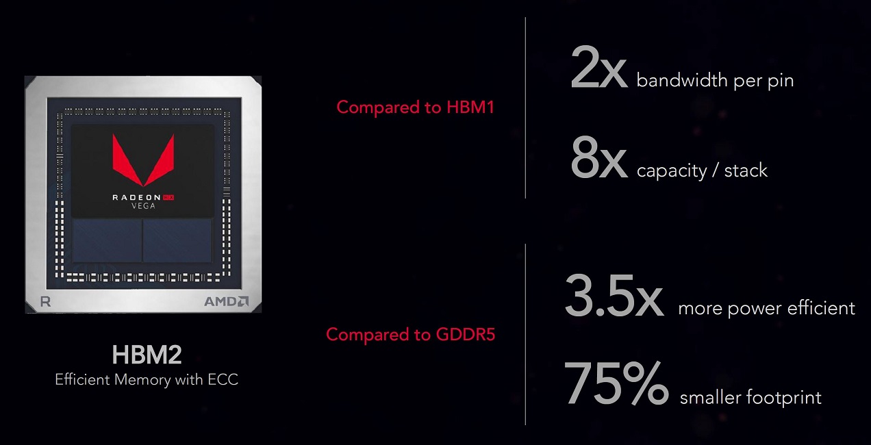
Vega is a big die and AMD helped here by marking clearly the sectors where the memory system is located. The biggest point regarding memory where Vega is considered is the introduction of HBM2 to the retail consumer market - 8 GB HBM2, which was otherwise only available in high-end professional development solutions costing an order of magnitude more. HBM2 has higher capacity per stack, which in turn increases the maximum memory capacity as well, relative to HBM1. AMD has also provided a comparison to GDDR5 (as opposed to GDDR5X, which is what NVIDIA uses in their competing GeForce solutions) to mention the higher efficiency and lower foot print. The latter holds true even with GDDR5X, however, as our RX Vega Preview indicates, so it has been for nought given the VGA card's PCB appears to be longer than what we had with the AMD R9 Fury series that first introduced HBM.

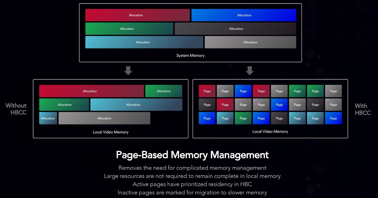


In order to best make use of the higher bandwidth available with HBM2, AMD's Radeon Technology Group (RTG) devised a brand new High-Bandwidth Cache Controller (HBCC) to help maximize GPU VRAM utilization through grouped memory. Here, VRAM is used as a cache device for system memory and/or disk storage, and HBCC controls data movement in an intelligent manner. As a quick visualization of how memory management is otherwise done, AMD is showing how HBCC can help with a page-based management system wherein data segments are handled individually rather than as complete chunks with active pages residing in the high-bandwidth cache and inactive pages in the slower memory.
This can be especially handy when a program loads into memory resources it finds relevant to the 3D scene being rendered without it needing access to them all for every single frame. This disparity hampers the otherwise high memory bandwidth and consumes resources moving said data. On large working sets, this also brings with it the chance that the physical GPU memory overflows, causing expensive swapping operations to happen in an unorganized manner. By using the high-bandwidth memory cache (HBMC) in Vega, AMD is tackling this via a direct hardware solution, and this is where the HBCC comes in.
The example above showed uniformly sized pages, but the high-bandwidth cache controller is designed to handle irregularly sized memory pages as well. Typical page sizes are between 4K and 128K. It can access not just system memory and storage, but non-volatile RAM as well, such as Intel's new Optane technology-based SSDs. If you have used a small SDD as a scratch/cache disk with a spinning drive, think of the practical benefits you achieved.
The design of the high-bandwidth cache controller will be handy also in that AMD now has a platform to use this concept with new microarchitectures or scaled-up silicon, and expand upon the same functionality. As it is now, it provides as much as 27 GB worth of assets to be used, allowing for real-time OpenGL rendering of ~500 million triangles. AMD estimates that this can be expanded upon to as much as 512 TB of virtual space.
Next Generation Compute Unit

Call it GCN 5.0, or GCN 1.6, or even Next Gen GCN, it is clear that Vega builds upon the existing GCN microarchitecture with some improvements added. AMD distinguishes this by referring to their compute units as "Next Generation Compute units" or NGCUs. This is where the bulk of the magic.. err.. the engineering has happened. AMD can not just turn its back on GCN because the architecture is used in millions of consoles, which helps developers port their tech to PC in a more time- and cost-efficient way.
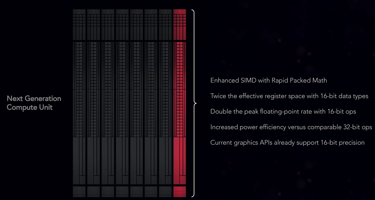
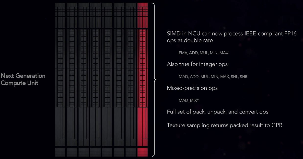
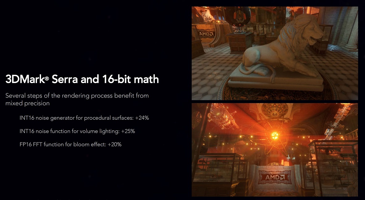
AMD has added support for 8-bit operations with NGCU, has retained the 16-bit floating point operations from Polaris, and continued to maintain FP32 and FP64 operation support as well. One new feature here is Rapid Packed Math wherein multiple 16-bit operations can be handled simultaneously between 32-bit operations. If a task has some complex 32-bit operations where precision is key, nothing changes. However, if your application is not demanding on precision - for example, if it is a lighting effect or change from one to another - you can use Rapid Packed Math to perform said operation as a 16-bit one, which has it take up less resources and increases performance throughput. AMD estimates a Vega NGCU to be able to handle 4-5x the number of operations per clock cycle relative to the previous CUs in Polaris. They demonstrate a usage case of Rapid Packed Math using 3DMark Serra - a custom demo created by Futuremark for AMD to show off this technology - wherein 16-bit integer and floating point operations result in as much as a 25% benefit in operation count.
AMD encourages developers to take a good look at their shaders and think where they need full 32-bit precision or why they can opt for 16-bit without losing any visual fidelity, but gaining significant performance improvements. For example, a noise-generating shader doesn't need 32-bit precision, 16-bit would be perfectly fine and still provides a value range large and differentiated enough for a decent noise effect.
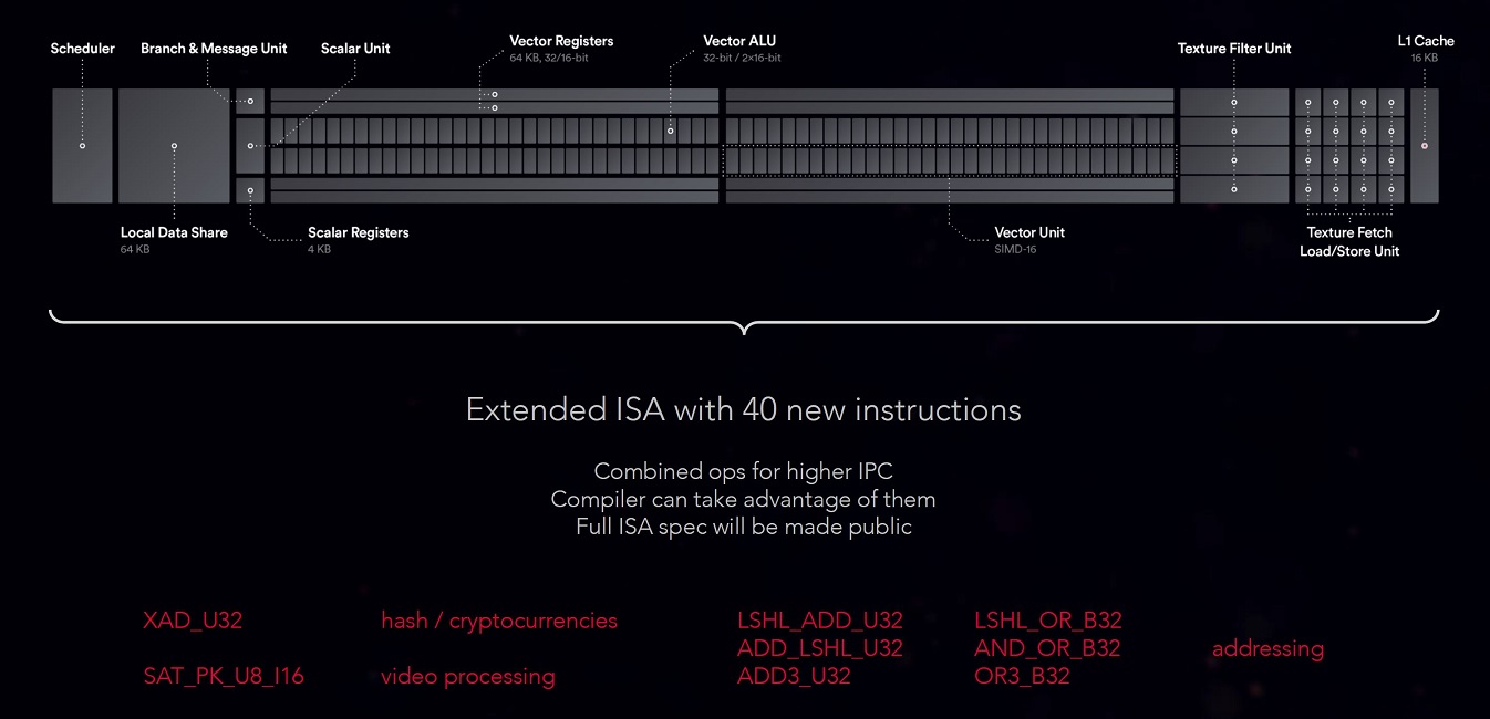
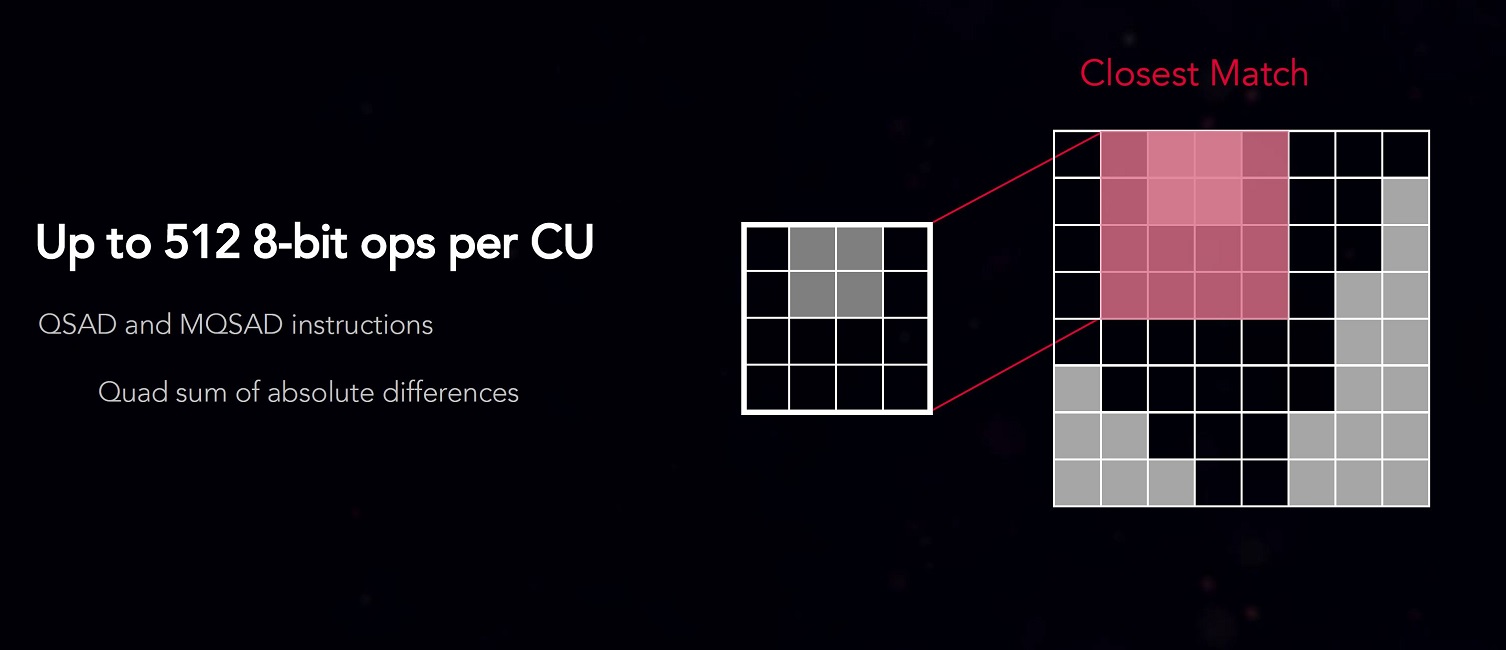
Aiding in computation with Vega NGCU is added support for over 40 new ISA instructions that take advantage also of the increased IPC over Polaris. Here's the thing - some of these are very relevant to GPU mining. Need I say more on where this goes? AMD estimates a single NGCU to be able to handle as many as 512 simultaneous 8-bit operations.
Our Patreon Silver Supporters can read articles in single-page format.
Apr 25th, 2024 09:04 EDT
change timezone
Latest GPU Drivers
New Forum Posts
- i7-12800HX Overheating Issues (2)
- (Anti) SFF fun house (354)
- What's your latest tech purchase? (20339)
- Intel ARC Firmware Compilation Matrix (22)
- Alphacool CORE 1 CPU block - bulging with danger of splitting? (6)
- Bizarre Throttlestop issue (6)
- Core i5-6300U (17)
- Last game you purchased? (255)
- Share your AIDA 64 cache and memory benchmark here (2916)
- What phone you use as your daily driver? And, a discussion of them. (1472)
Popular Reviews
- Fractal Design Terra Review
- Thermalright Phantom Spirit 120 EVO Review
- Corsair 2000D Airflow Review
- Minisforum EliteMini UM780 XTX (AMD Ryzen 7 7840HS) Review
- ASUS GeForce RTX 4090 STRIX OC Review
- NVIDIA GeForce RTX 4090 Founders Edition Review - Impressive Performance
- ASUS GeForce RTX 4090 Matrix Platinum Review - The RTX 4090 Ti
- MSI GeForce RTX 4090 Suprim X Review
- MSI GeForce RTX 4090 Gaming X Trio Review
- Gigabyte GeForce RTX 4090 Gaming OC Review
Controversial News Posts
- Sony PlayStation 5 Pro Specifications Confirmed, Console Arrives Before Holidays (116)
- NVIDIA Points Intel Raptor Lake CPU Users to Get Help from Intel Amid System Instability Issues (106)
- AMD "Strix Halo" Zen 5 Mobile Processor Pictured: Chiplet-based, Uses 256-bit LPDDR5X (101)
- US Government Wants Nuclear Plants to Offload AI Data Center Expansion (98)
- Windows 11 Now Officially Adware as Microsoft Embeds Ads in the Start Menu (87)
- Developers of Outpost Infinity Siege Recommend Underclocking i9-13900K and i9-14900K for Stability on Machines with RTX 4090 (85)
- Windows 10 Security Updates to Cost $61 After 2025, $427 by 2028 (84)
- AMD's RDNA 4 GPUs Could Stick with 18 Gbps GDDR6 Memory (81)