 88
88
ASUS GeForce GTX 570 Review
(88 Comments) »GTX 570 Review Introduction
Last month, NVIDIA made an impactful product launch, the GeForce GTX 580, which shook the GPU world and tilted performance leadership and performance per Watt figures back in favor of NVIDIA. Such was its impact that it may have caused its competitor to delay upcoming product launches to probably rework them up. Not very far from the launch of those products, NVIDIA launched its second GPU in the GeForce 500 series, the GeForce GTX 570. As the name would suggest, this is the "value" SKU based on the GF110 GPU, while the GTX 580 leads with all components of the GPU enabled.

Reviewed today, the GeForce GTX 570 is GF110 with one streaming multiprocessor (SM) disabled, yielding 480 CUDA cores (same number as that of the GTX 480 from the previous generation), but with a 320-bit GDDR5 memory interface, connecting to 1280 MB of memory. The ROP as a result is 40. Thanks to the improved power efficiency, NVIDIA was able to up clock speeds over the previous generation without having to worry about rising TDP. The core is clocked at 732 MHz (higher than that of GTX 480), CUDA cores at 1464 MHz (again, higher than that of GTX 480, translating into higher shader compute power), and 950 MHz (3800 MHz GDDR5 effective) memory, yielding 152 GB/s of memory bandwidth. To top it off, the board power is rated at 219W, and power is drawn in from two 6-pin power connectors.
| GeForce GTX 460 | GeForce GTX 460 | Radeon HD 6850 | Radeon HD 5850 | GeForce GTX 470 | Radeon HD 6870 | Radeon HD 5870 | GeForce GTX 570 | ASUS GeForce GTX 570 | GeForce GTX 480 | GeForce GTX 580 | Radeon HD 5970 | |
| Shader units | 336 | 336 | 960 | 1440 | 448 | 1120 | 1600 | 480 | 480 | 480 | 512 | 2x 1600 |
| ROPs | 24 | 32 | 32 | 32 | 40 | 32 | 32 | 40 | 40 | 48 | 48 | 2x 32 |
| GPU | GF104 | GF104 | Barts | Cypress | GF100 | Barts | Cypress | GF110 | GF110 | GF100 | GF110 | 2x Cypress |
| Transistors | 1950M | 1950M | 1700M | 2154M | 3200M | 1700M | 2154M | 3000M | 3000M | 3200M | 3000M | 2x 2154M |
| Memory Size | 768 MB | 1024 MB | 1024 MB | 1024 MB | 1280 MB | 1024 MB | 1024 MB | 1280 MB | 1280 MB | 1536 MB | 1536 MB | 2x 1024 MB |
| Memory Bus Width | 192 bit | 256 bit | 256 bit | 256 bit | 320 bit | 256 bit | 256 bit | 320 bit | 320 bit | 384 bit | 384 bit | 2x 256 bit |
| Core Clock | 675 MHz | 675 MHz | 775 MHz | 725 MHz | 607 MHz | 900 MHz | 850 MHz | 732 MHz | 742 MHz | 700 MHz | 772 MHz | 725 MHz |
| Memory Clock | 900 MHz | 900 MHz | 1000 MHz | 1000 MHz | 837 MHz | 1050 MHz | 1200 MHz | 950 MHz | 950 MHz | 924 MHz | 1002 MHz | 1000 MHz |
| Price | $160 | $200 | $180 | $260 | $260 | $240 | $360 | $330 | $330 | $450 | $500 | $580 |
The Card
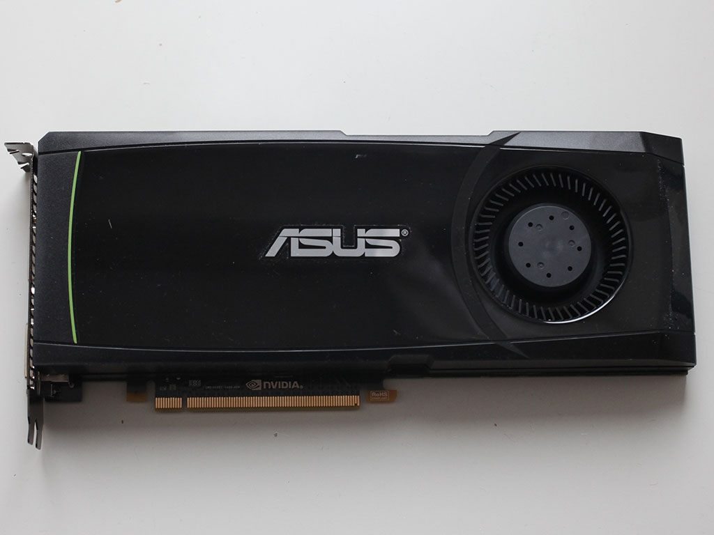

ASUS' GeForce GTX 570 looks exactly like the Geforce GTX 580, even the stickers are in the same position.

NVIDIA's GeForce GTX 570 requires two slots in your system.
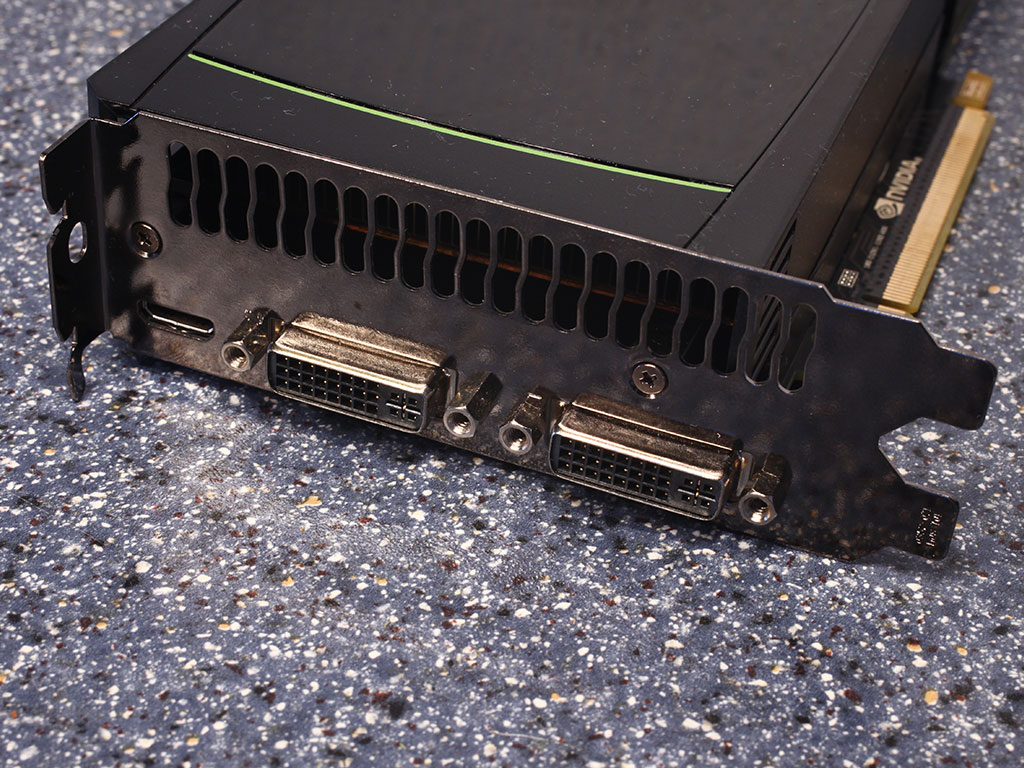
The card has two DVI ports and one one mini-HDMI port. According to NVIDIA the card also supports DisplayPort if board partners want to use it. Unlike AMD's latest GPUs, the output logic design is not as flexible. On AMD cards vendors are free to combine six TMDS links into any output configuration they want (dual-link DVI consuming two links), on NVIDIA, you are fixed to two DVI outputs and one HDMI/DP in addition to that. NVIDIA confirmed that you can use only two displays at the same time, so for a three monitor setup you would need two cards.
NVIDIA has included an HDMI sound device inside their GPU which does away with the requirement of connecting an external audio source to the card for HDMI audio. The HDMI interface is HDMI 1.3a compatible which includes Dolby TrueHD, DTS-HD, AC-3, DTS and up to 7.1 channel audio with 192 kHz / 24-bit. NVIDIA also claims full support for the 3D portion of the HDMI 1.4 specification which will become important later this year when we will see first Blu-Ray titles shipping with support for 3D output.

You may combine up to four GeForce GTX 570 cards in SLI for increased performance or improved image quality settings.


Here are the front and the back of the card, high-res versions are also available (front, back). If you choose to use these images for voltmods etc, please include a link back to this site or let us post your article.
A Closer Look


The GeForce GTX 570 & 580 are some of the few graphics cards that use a vapor-chamber technology heatplate to maximize heat transfer between the GPU and the rest of the heatsink. You can also see above that the heatsink cools secondary components like voltage regulation circuitry and memory chips. Overall this seems to be a very capable thermal solution but that also increases its price.

Instead of the 6+8 power configuration on the GeForce GTX 580, ASUS has chosen a 6+6 PCI-Express power setup which is sufficient for this card.


In order to stay within the 300 W power limit, NVIDIA has added a power draw limitation system to their GTX 570 and GTX 580. When either Furmark or OCCT are detected running by the driver, three Texas Instruments INA219 sensors measure the inrush current and voltage on all 12 V lines (PCI-E slot, 6-pin, 8-pin) to calculate power. As soon as the power draw exceeds a predefined limit, the card will automatically clock down and restore clocks as soon as the overcurrent situation has gone away. NVIDIA emphasizes this is to avoid damage to cards or motherboards from these stress testing applications and claims that in normal games and applications such an overload will not happen. I am still concerned that with heavy overclocking, especially on water and LN2 the limiter might engage, and reduce clocks which results in reduced performance. Real-time clock monitoring does not show the changed clocks, so besides the loss in performance it could be difficult to detect that state without additional testing equipment or software support.
The second picture shows the jumps in power consumption over time while running Furmark. Compared to the GeForce GTX 580, it seems that the card can now enter several low-frequency states whereas on the GTX 580 it could only reduce the clock speed by 50%.
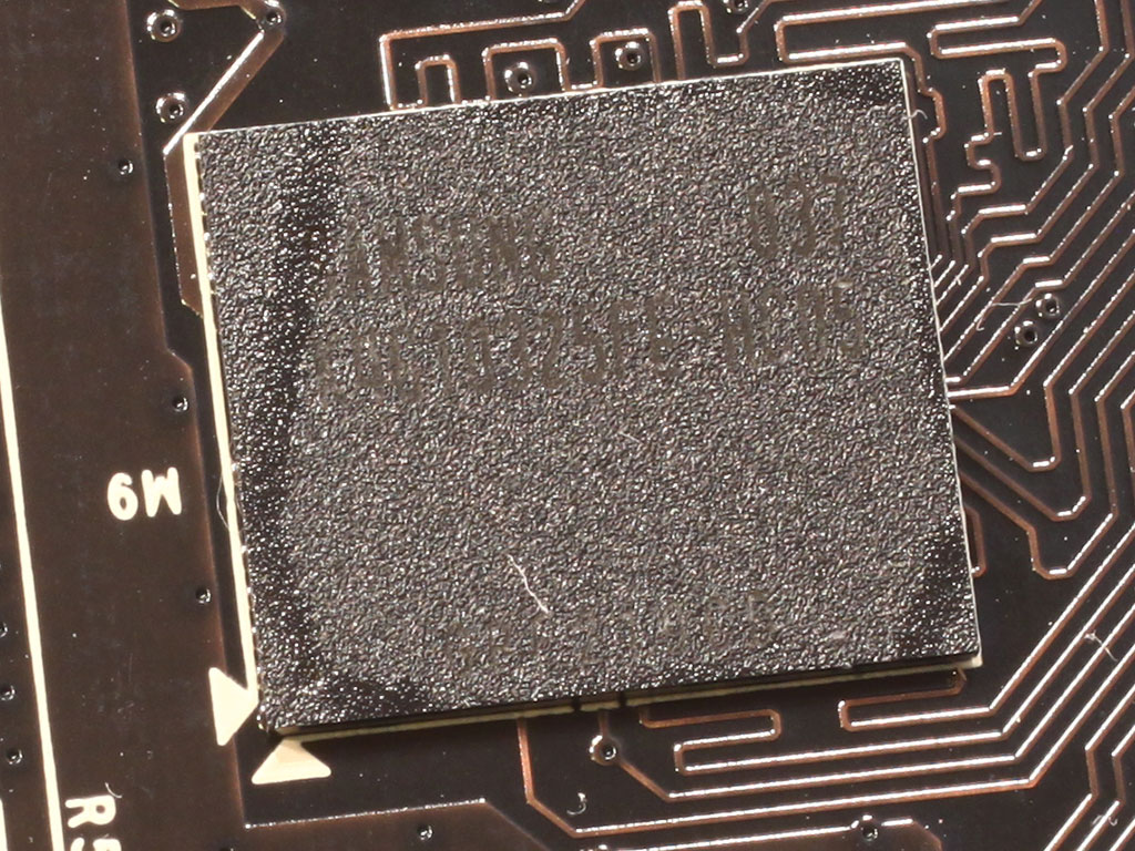
The GDDR5 memory chips are made by Samsung, and carry the model number K4G10325FE-HC04. They are specified to run at 1250 MHz (5000 MHz GDDR5 effective).

Just like on the GeForce GTX 480 and 580, NVIDIA uses a CHiL CHL 8266 voltage regulator on their card. This controller offers extensive monitoring and voltage control options via I2C, so it's a great choice for overclockers.

NVIDIA's GeForce 110 graphics processor is made on a 40 nm process at TSMC Taiwan. It uses approximately 3.0 billion transistors which is 200 million less than the GF100. Please note that the silvery metal surface you see is the heatspreader of the GPU. The actual GPU die is sitting under the heatspreader. According to NVIDIA, the die size of the GF110 graphics processor is 520 mm².
Test System
| Test System - VGA Rev. 12 | |
|---|---|
| CPU: | Intel Core i7 920 @ 3.8 GHz (Bloomfield, 8192 KB Cache) |
| Motherboard: | Gigabyte X58 Extreme Intel X58 & ICH10R |
| Memory: | 3x 2048 MB Mushkin Redline XP3-12800 DDR3 @ 1520 MHz 8-7-7-16 |
| Harddisk: | WD Caviar Black 6401AALS 640 GB |
| Power Supply: | akasa 1200W |
| Software: | Windows 7 64-bit |
| Drivers: | GTX 570 & 580: 263.09 NVIDIA: 260.99 ATI: Catalyst 10.11 |
| Display: | LG Flatron W3000H 30" 2560x1600 |
- All video card results were obtained on this exact system with the exact same configuration.
- All games were set to their highest quality setting
- 1024 x 768, No Anti-aliasing. This is a standard resolution without demanding display settings.
- 1280 x 1024, 2x Anti-aliasing. Common resolution for most smaller flatscreens today (17" - 19"). A bit of eye candy turned on in the drivers.
- 1680 x 1050, 4x Anti-aliasing. Most common widescreen resolution on larger displays (19" - 22"). Very good looking driver graphics settings.
- 1920 x 1200, 4x Anti-aliasing. Typical widescreen resolution for large displays (22" - 26"). Very good looking driver graphics settings.
- 2560 x 1600, 4x Anti-aliasing. Highest possible resolution for commonly available displays (30"). Very good looking driver graphics settings.
Our Patreon Silver Supporters can read articles in single-page format.
Apr 19th, 2024 23:55 EDT
change timezone
Latest GPU Drivers
New Forum Posts
- Liquidextasy waterblocks (51)
- I just succesfully baked DDR4 (76)
- GPU-Z reporting wrong ReBar info for RTX 20 series (4)
- I9 13890HX undervolting Suggestions (5)
- Official Board Game Discussion (4)
- Roccat Kone AIMO has developed a double left click, when I click it once. Any fix out there? (37)
- Cinebench crashed my PC. My Wi-Fi stopped working, and I keep getting a "Please wait" screen when I boot up my PC. (8)
- USB C to USB A hub (43)
- XFX RX580 stock Bios (8)
- Your PC ATM (34488)
Popular Reviews
- Horizon Forbidden West Performance Benchmark Review - 30 GPUs Tested
- Fractal Design Terra Review
- Corsair 2000D Airflow Review
- Thermalright Phantom Spirit 120 EVO Review
- Minisforum EliteMini UM780 XTX (AMD Ryzen 7 7840HS) Review
- Creative Pebble X Plus Review
- FiiO KB3 HiFi Mechanical Keyboard Review - Integrated DAC/Amp!
- ASUS GeForce RTX 4090 STRIX OC Review
- NVIDIA GeForce RTX 4090 Founders Edition Review - Impressive Performance
- ASUS GeForce RTX 4090 Matrix Platinum Review - The RTX 4090 Ti
Controversial News Posts
- Sony PlayStation 5 Pro Specifications Confirmed, Console Arrives Before Holidays (111)
- NVIDIA Points Intel Raptor Lake CPU Users to Get Help from Intel Amid System Instability Issues (102)
- US Government Wants Nuclear Plants to Offload AI Data Center Expansion (98)
- AMD "Strix Halo" Zen 5 Mobile Processor Pictured: Chiplet-based, Uses 256-bit LPDDR5X (84)
- Windows 10 Security Updates to Cost $61 After 2025, $427 by 2028 (82)
- Developers of Outpost Infinity Siege Recommend Underclocking i9-13900K and i9-14900K for Stability on Machines with RTX 4090 (82)
- TechPowerUp Hiring: Reviewers Wanted for Motherboards, Laptops, Gaming Handhelds and Prebuilt Desktops (73)
- Intel Realizes the Only Way to Save x86 is to Democratize it, Reopens x86 IP Licensing (70)