 21
21
ASUS GTX 750 Ti OC 2 GB Review
(21 Comments) »Introduction
Here it is, NVIDIA's GeForce GTX 750 Ti, one of the first GPUs based on its next-generation "Maxwell" GPU architecture. First reports of the chip being based on "Maxwell" hit us by surprise as we presumed that a new micro-architecture is invariably pegged to NVIDIA's foundry partner, TSMC, to launch its next-generation 20 nanometer silicon fabrication process. The fact that TSMC's 20 nm node isn't in a position to ship out such complex ASICs as graphics processors right now and that NVIDIA wouldn't want its new architecture to in any way be hit by unforeseen issues arising out of the move to a new process may have led to the decision to use the existing 28 nanometer process.
The GeForce GTX 750 Ti and GTX 750 (also launched today) are based on the 28 nm GM107 (GeForce-Maxwell 107) silicon. This 1.87 billion-transistor GPU features a basic component hierarchy that's not too different from that of "Kepler," but sees some under-the-hood changes in the design of its key parallel processing sub-unit, the streaming multiprocessor "Maxwell" (SMM). The GTX 750 Ti is positioned between the GTX 760 and GTX 660, which is a sizable gap to fill. NVIDIA is promising some huge performance-per-watt gains with "Maxwell." Given that the GM107 is based on the same 28 nm process as the GeForce Kepler series, there's only one way NVIDIA can deliver on its promise - by developing a better overall architecture.

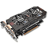
Today we are reviewing the ASUS GTX 750 Ti OC. This will be our first review of a GTX 750 Ti with a 6-pin power connector.
ASUS has also overclocked the card out of the box and uses their DirectCU dual-fan thermal solution on the card, but without heatpipes.
The card is currently available online for $160, which is a $10 price premium over the reference design.
| GeForce GTX 650 Ti | Radeon HD 7790 | Radeon HD 7850 | GeForce GTX 750 | Radeon R7 260X | GTX 650 Ti Boost | GeForce GTX 750 Ti | ASUS GTX 750 Ti OC | Radeon R7 265 | GeForce GTX 660 | Radeon HD 7870 | Radeon R9 270X | GeForce GTX 660 Ti | GeForce GTX 760 | |
|---|---|---|---|---|---|---|---|---|---|---|---|---|---|---|
| Shader Units | 768 | 896 | 1024 | 512 | 896 | 768 | 640 | 640 | 1024 | 960 | 1280 | 1280 | 1344 | 1152 |
| ROPs | 16 | 16 | 32 | 16 | 16 | 24 | 16 | 16 | 32 | 24 | 32 | 32 | 24 | 32 |
| Graphics Processor | GK106 | Bonaire | Pitcairn | GM107 | Bonaire | GK106 | GM107 | GM107 | Pitcairn | GK106 | Pitcairn | Pitcairn | GK104 | GK104 |
| Transistors | 2540M | 2080M | 2800M | 1870M | 2080M | 2540M | 1870M | 1870M | 2800M | 2540M | 2800M | 2800M | 3500M | 3500M |
| Memory Size | 1024 MB | 1024 MB | 2048 MB | 1024 MB | 2048 MB | 2048 MB | 2048 MB | 2048 MB | 2048 MB | 2048 MB | 2048 MB | 2048 MB | 2048 MB | 2048 MB |
| Memory Bus Width | 128 bit | 128 bit | 256 bit | 128 bit | 128 bit | 192 bit | 128 bit | 128 bit | 256 bit | 192 bit | 256 bit | 256 bit | 192 bit | 256 bit |
| Core Clock | 925 MHz | 1000 MHz | 860 MHz | 1020 MHz+ | 1100 MHz | 980 MHz+ | 1020 MHz+ | 1072 MHz+ | 925 MHz | 980 MHz+ | 1000 MHz | 1050 MHz | 915 MHz+ | 980 MHz+ |
| Memory Clock | 1350 MHz | 1500 MHz | 1200 MHz | 1250 MHz | 1625 MHz | 1502 MHz | 1350 MHz | 1350 MHz | 1400 MHz | 1502 MHz | 1200 MHz | 1400 MHz | 1502 MHz | 1502 MHz |
| Price | $100 | $115 | $150 | $120 | $130 | $130 | $150 | $160 | $150 | $190 | $190 | $200 | $260 | $240 |
Architecture
NVIDIA's primary design goal with the GM107 is to up the performance-per-watt game. If NVIDIA achieves a significant performance-per-watt gain with "Maxwell" over "Kepler," it can trade that gain for performance on bigger "Maxwell" chips bolstered by the 20 nm process. It's this fact that makes the GK107 academically interesting.As we mentioned earlier, the GM107 essentially features the same component hierarchy as previous generation "Kepler" GPUs, but introduces changes to the design of the streaming multiprocessor (SMM), the parallel-processing sub-unit of the GPU. At its outermost ring, the GM107 features the GigaThread Engine, a component that marshals data and instructions between the graphics processing cluster (GPC), the raster operations processors (ROPs), the L3 cache, the memory controllers, the bus interface, and the display I/O.
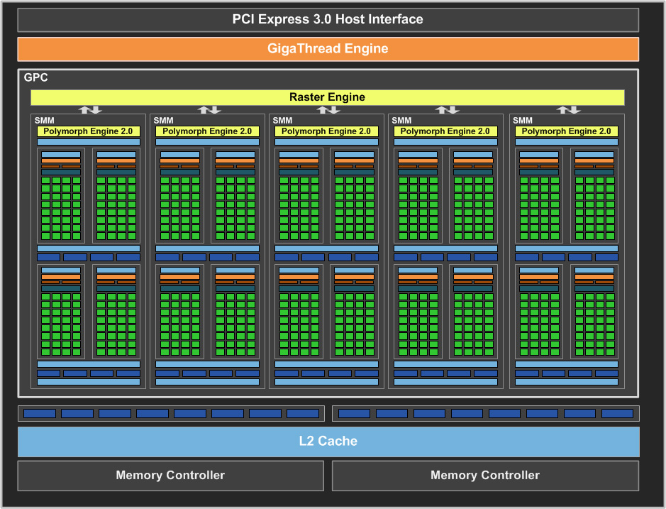
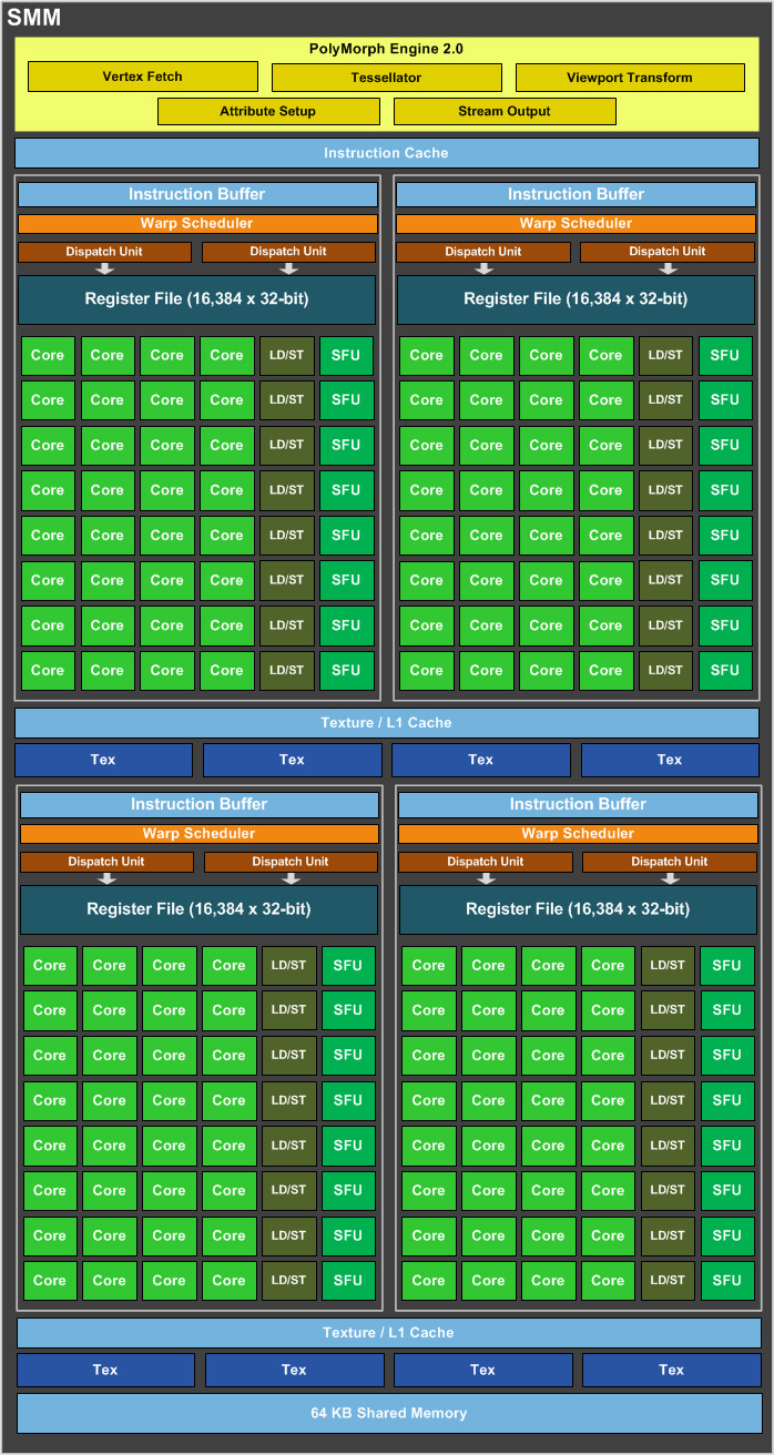
Several GPCs can typically be routed to a GigaThread engine, but being a mid-range GPU, the GM107 features just one. This GPC features a raster engine that handles high-level assembly of data and instructions and five streaming multiprocessors (SMMs), which is where the number crunching takes place. Unlike the streaming multiprocessors (SMXs) of "Kepler" GPUs, which feature an incoherent group of 192 CUDA cores, the SMM features four groups of 32 cores each, which totals 128 per SMM. The SMM shares a Polymorph Engine that features components such as the tessellator, fetch, setup, transform, and stream output with the four groups. The four groups of 32 CUDA cores, each, feature dedicated warp schedulers and registers, with a texture cache cushioning transfers between the groups and TMUs. The GM107 hence features a total of 640 CUDA cores and 48 TMUs. At a higher level, the chip features 16 color ROPs and a 128-bit wide GDDR5 memory interface.
Packaging


Contents

You will receive:
- Graphics card
- Driver CD + documentation
Our Patreon Silver Supporters can read articles in single-page format.
Apr 19th, 2024 21:16 EDT
change timezone
Latest GPU Drivers
New Forum Posts
- Dell Workstation Owners Club (3051)
- I brought my old screen-less laptop to new life (0)
- Your PC ATM (34487)
- I just succesfully baked DDR4 (72)
- Roccat Kone AIMO has developed a double left click, when I click it once. Any fix out there? (35)
- Windows 11 General Discussion (5014)
- GTX 1060 6GB ASUS GPU Shuts Down after 5min of Gaming (4)
- Official Board Game Discussion (1)
- USB C to USB A hub (42)
- The Official Linux/Unix Desktop Screenshots Megathread (688)
Popular Reviews
- Horizon Forbidden West Performance Benchmark Review - 30 GPUs Tested
- Fractal Design Terra Review
- Corsair 2000D Airflow Review
- Thermalright Phantom Spirit 120 EVO Review
- Minisforum EliteMini UM780 XTX (AMD Ryzen 7 7840HS) Review
- Creative Pebble X Plus Review
- FiiO KB3 HiFi Mechanical Keyboard Review - Integrated DAC/Amp!
- ASUS GeForce RTX 4090 STRIX OC Review
- NVIDIA GeForce RTX 4090 Founders Edition Review - Impressive Performance
- ASUS GeForce RTX 4090 Matrix Platinum Review - The RTX 4090 Ti
Controversial News Posts
- Sony PlayStation 5 Pro Specifications Confirmed, Console Arrives Before Holidays (111)
- NVIDIA Points Intel Raptor Lake CPU Users to Get Help from Intel Amid System Instability Issues (102)
- US Government Wants Nuclear Plants to Offload AI Data Center Expansion (98)
- AMD "Strix Halo" Zen 5 Mobile Processor Pictured: Chiplet-based, Uses 256-bit LPDDR5X (84)
- Windows 10 Security Updates to Cost $61 After 2025, $427 by 2028 (82)
- Developers of Outpost Infinity Siege Recommend Underclocking i9-13900K and i9-14900K for Stability on Machines with RTX 4090 (82)
- TechPowerUp Hiring: Reviewers Wanted for Motherboards, Laptops, Gaming Handhelds and Prebuilt Desktops (72)
- Intel Realizes the Only Way to Save x86 is to Democratize it, Reopens x86 IP Licensing (70)