 122
122
ASUS Radeon RX 5700 XT STRIX OC Review
(122 Comments) »Introduction
ASUS today launched the first fully custom-design Radeon RX 5700 XT graphics card, the Republic of Gamers STRIX RX 5700 XT OC. The company leads a string of custom-design Radeon RX 5700 series "Navi" graphics card launches from AMD's add-in board partners a little over a month after AMD debuted this 7 nm GPU on 7/7 (7th July). The RX 5700 XT and its sibling, the RX 5700, have until today only been available in AMD's reference-design boards.
The Radeon RX 5700 XT is AMD's first true performance-segment graphics card in over two years since the RX Vega series. It's based on the brand new "Navi" architecture that leverages the 7 nm silicon fabrication process and brand new number-crunching machinery AMD calls RDNA compute units. These constitute the biggest update to AMD's GPU design since the very first Graphics CoreNext (GCN) architecture circa 2013. Together with clock speeds, RDNA is designed to bring about massive IPC improvements over GCN. The silicon also has a number of architectural changes. An interesting series of price adjustments and product launches ensures that even at its starting price of $399, it offers a bit more price-performance than NVIDIA.

AMD had originally planned to launch the Radeon RX 5700 XT at $449 and the RX 5700 at $399, with the two cards beating the $499 NVIDIA RTX 2070 and $349 RTX 2060, respectively. This forced NVIDIA to refresh its lineup with the new RTX 2070 Super at $499 and the RTX 2060 Super at $399. The RTX 2060 Super in particular was carefully crafted not to cannibalize the RTX 2070. AMD seeped into this imbroglio of NVIDIA and slotted the RX 5700 XT at $399 and the RX 5700 at $349, at which they outclass the RTX 2060 Super and original RTX 2060, respectively. NVIDIA didn't adjust prices of its RTX 2060 Super or RTX 2070 Super any further, and we hence have a fair bit of headroom between the RTX 2060 Super and RTX 2070 Super, in which AMD's board partners can launch custom-design RX 5700 XT cards with factory-overclocked speeds and other goodies, such as quieter coolers.
At the heart of the Radeon RX 5700 XT is the 7 nm "Navi 10" silicon with an impressive 10.3 billion transistors crammed into a 251 mm² die. Unlike the "Vega 20," Navi is a more traditional GPU in that the package only has the GPU die and is surrounded by memory chips. AMD opted for cost-effective 256-bit GDDR6 memory over exotic design choices such as HBM2. At a memory frequency of 14 Gbps, Navi enjoys a healthy memory bandwidth of 448 GB/s. It also features the latest-generation PCI-Express gen 4.0 x16 host interface with full backwards compatibility for older generations of PCIe, which means you can pair it with AMD's new Ryzen 3000 processors on an X570 chipset motherboard. The buzz-words "7 nm" and "PCIe gen 4.0" are extensively used in AMD's marketing, as if to suggest that Navi is a generation ahead of NVIDIA's Turing, which is built on 12 nm and has PCIe gen 3.0.
The ASUS ROG STRIX RX 5700 XT OC features a custom-design PCB designed by ASUS with a massive 14-phase VRM that draws power from a pair of 8-pin PCIe power connectors, and several goodies, such as a digital RGB header, a couple of PWM case-fan headers, voltage measurement points for pro-users, and more. The cooling solution is the ASUS DirectCU III, the latest in a long line of high-end air-based cooling solutions from ASUS that features an aluminium fin-stack heatsink and a trio of fans that turn off when the GPU is idling. Better cooling and power limits mean that the GPU is able to sustain its boost clock speeds better, resulting in more performance. There's also a software-enabled OC mode that dials up boost clock speeds to 2035 MHz. The dual-BIOS feature not only prevents you from paying the noob tax, but also lets you lower fan speeds via a "quiet BIOS." Living true to the ROG STRIX brand, this card has a healthy dose of RGB LED embellishments along the front, top, and back of the card. ASUS hasn't revealed the pricing of this card yet. We will update the review when we have it.
| Price | Shader Units | ROPs | Core Clock | Boost Clock | Memory Clock | GPU | Transistors | Memory | |
|---|---|---|---|---|---|---|---|---|---|
| GTX 1070 Ti | $450 | 2432 | 64 | 1607 MHz | 1683 MHz | 2000 MHz | GP104 | 7200M | 8 GB, GDDR5, 256-bit |
| RTX 2060 | $290 | 1920 | 48 | 1365 MHz | 1680 MHz | 1750 MHz | TU106 | 10800M | 6 GB, GDDR6, 192-bit |
| RX 5700 | $350 | 2304 | 64 | 1465 MHz | 1625 MHz | 1750 MHz | Navi 10 | 10300M | 8 GB, GDDR6, 256-bit |
| GTX 1080 | $500 | 2560 | 64 | 1607 MHz | 1733 MHz | 1251 MHz | GP104 | 7200M | 8 GB, GDDR5X, 256-bit |
| RTX 2060 Super | $400 | 2176 | 64 | 1470 MHz | 1650 MHz | 1750 MHz | TU106 | 10800M | 8 GB, GDDR6, 256-bit |
| RX Vega 64 | $400 | 4096 | 64 | 1247 MHz | 1546 MHz | 953 MHz | Vega 10 | 12500M | 8 GB, HBM2, 2048-bit |
| GTX 1080 Ti | $700 | 3584 | 88 | 1481 MHz | 1582 MHz | 1376 MHz | GP102 | 12000M | 11 GB, GDDR5X, 352-bit |
| RX 5700 XT | $400 | 2560 | 64 | 1605 MHz | 1755 MHz | 1750 MHz | Navi 10 | 10300M | 8 GB, GDDR6, 256-bit |
| ASUS RX 5700 XT STRIX OC | Unknown | 2560 | 64 | 1770 MHz | 1905 MHz | 1750 MHz | Navi 10 | 10300M | 8 GB, GDDR6, 256-bit |
| RTX 2070 | $440 | 2304 | 64 | 1410 MHz | 1620 MHz | 1750 MHz | TU106 | 10800M | 8 GB, GDDR6, 256-bit |
| RTX 2070 Super | $500 | 2560 | 64 | 1605 MHz | 1770 MHz | 1750 MHz | TU104 | 13600M | 8 GB, GDDR6, 256-bit |
| Radeon VII | $680 | 3840 | 64 | 1802 MHz | N/A | 1000 MHz | Vega 20 | 13230M | 16 GB, HBM2, 4096-bit |
| RTX 2080 | $630 | 2944 | 64 | 1515 MHz | 1710 MHz | 1750 MHz | TU104 | 13600M | 8 GB, GDDR6, 256-bit |
Architecture: Navi and RDNA


We've been hearing the moniker "Navi" for years now, and AMD threw another one at us this Computex, "RDNA", so let us demystify the two first. "Navi" is the codename for the family of silicon the GPU is based on. RDNA is a new architecture introduced by AMD to succeed Graphics Core Next (GCN). It prescribes the GPU's component hierarchy and, more importantly, its main number-crunching machinery, the compute units.
Another example of this distinction would be "Vega". Vega 10, Vega 20, and Vega 12 are pieces of silicon from the same family, while the GPU follows the 5th generation Graphics Core Next architecture governing even its compute units. Over many years, AMD made incremental updates to GCN, but this time, it claims that RDNA is sufficiently different from GCN to not be considered a new version, but rather a new hardware component that brings with it massive IPC gains over the previous generation.


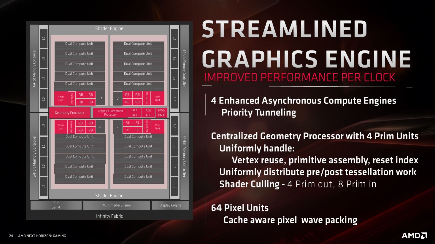
The Radeon RX 5700 series is built around "Navi 10", an elegant little piece of silicon engineered on the 7 nm process at TSMC with 10.3 billion transistors crammed into a die measuring just 251 mm². The chip features a PCI-Express 4.0 x16 bus interface and a 256-bit wide GDDR6 memory interface. Infinity Fabric, which debuted on AMD's Ryzen CPUs, is extensively used as an on-die interconnect linking the various major components.
The bulk of AMD's engineering effort with RDNA has been to increase the number of dedicated resources to avoid starvation by fewer components waiting for access to a resource. The "Navi 10" silicon has two Shader Engines sharing a centralized Command Processor that distributes workloads, a Geometry Processor, and ACEs (asynchronous compute engines).


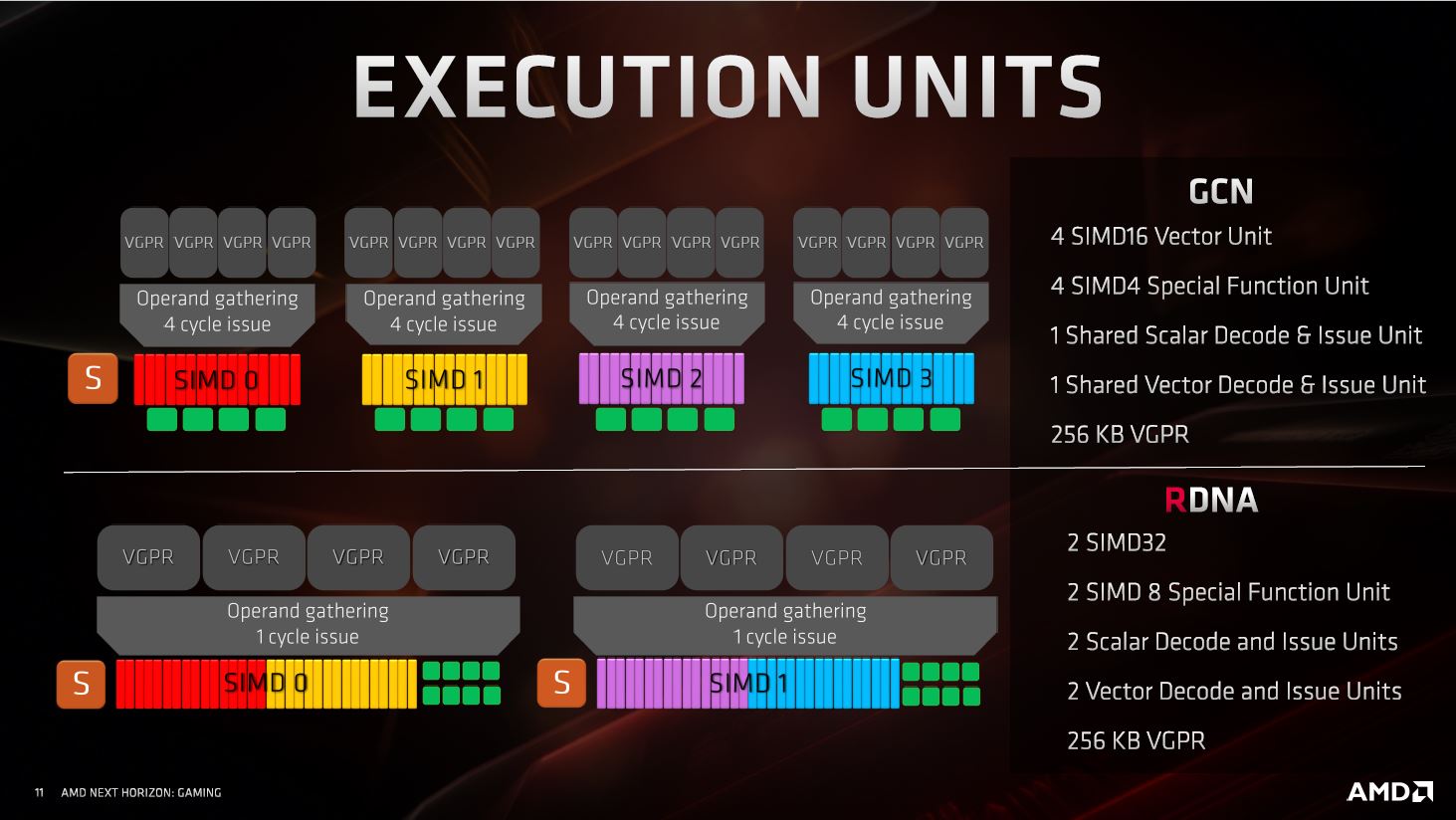
Each Shader Engine is further divided into two Graphics Engines. A graphics engine shares render backends, a Rasterizer, and a Prim Unit among five Workgroup Processors. This is where the core of RDNA begins. AMD figured it could merge two compute units (CUs) to share schedulers, scalar units, a data-share, instruction and data caches, and TMUs. The Workgroup Processor, or "dual-compute unit" as shown in the architecture block diagram, is for all intents and purposes indivisible in that individual CUs cannot be disabled.
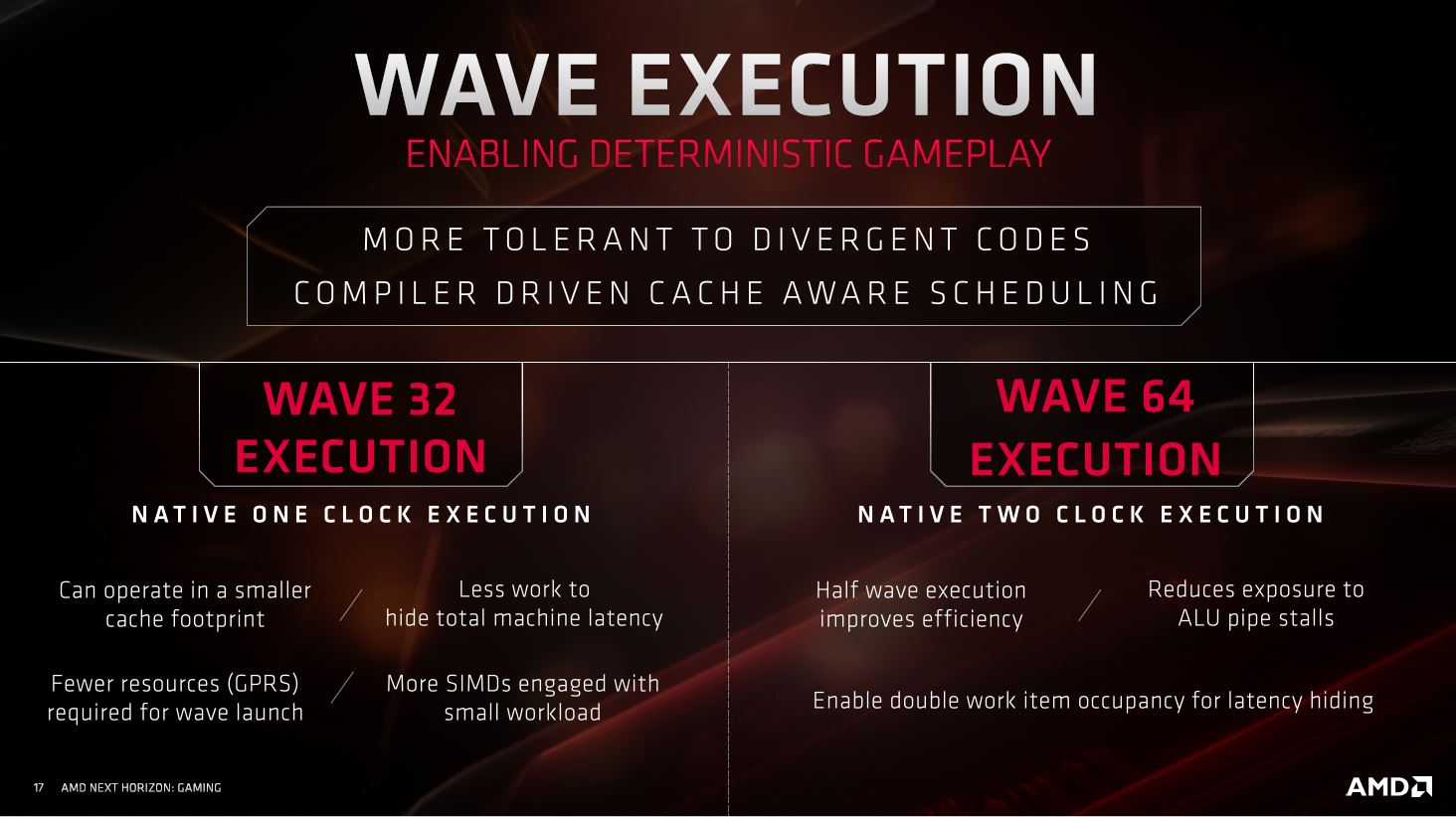

An RDNA compute unit packs 64 stream processors for vector operations and double the number of scalar units for localized serial processing. The stream processors in a CU are split into groups of two, each equipped with a scalar unit. According to AMD, this greatly reduces latency and improves the overall IPC of the compute unit. It also more efficiently utilizes local caches.

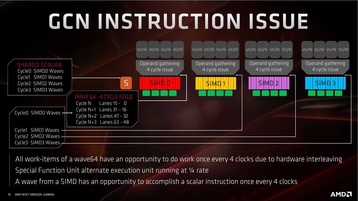
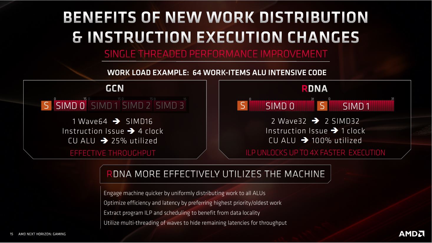
The vector execution units, or stream processors, are where much of the GPU's parallel processing happens. Due to the redesigned compute unit, two scalar processors pull two SIMD32 vector units made up of 32 stream processors, each, instead of a single scalar processor pulling four SIMD16 vector units. How is this important? On GCN, the way SIMD units are laid out, all items in a Wave64 operation get to do work once every four clocks due to hardware interleaving. With RDNA, Wave32 work items can do work every clock cycle. In all, RDNA minimizes wasted clock cycles by more efficiently and uniformly utilizing the hardware resources.
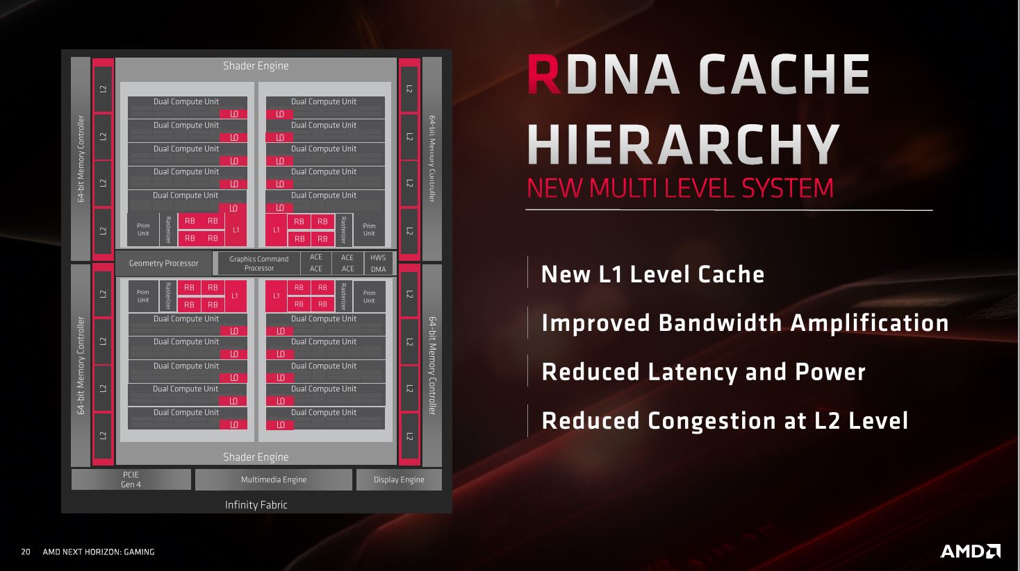


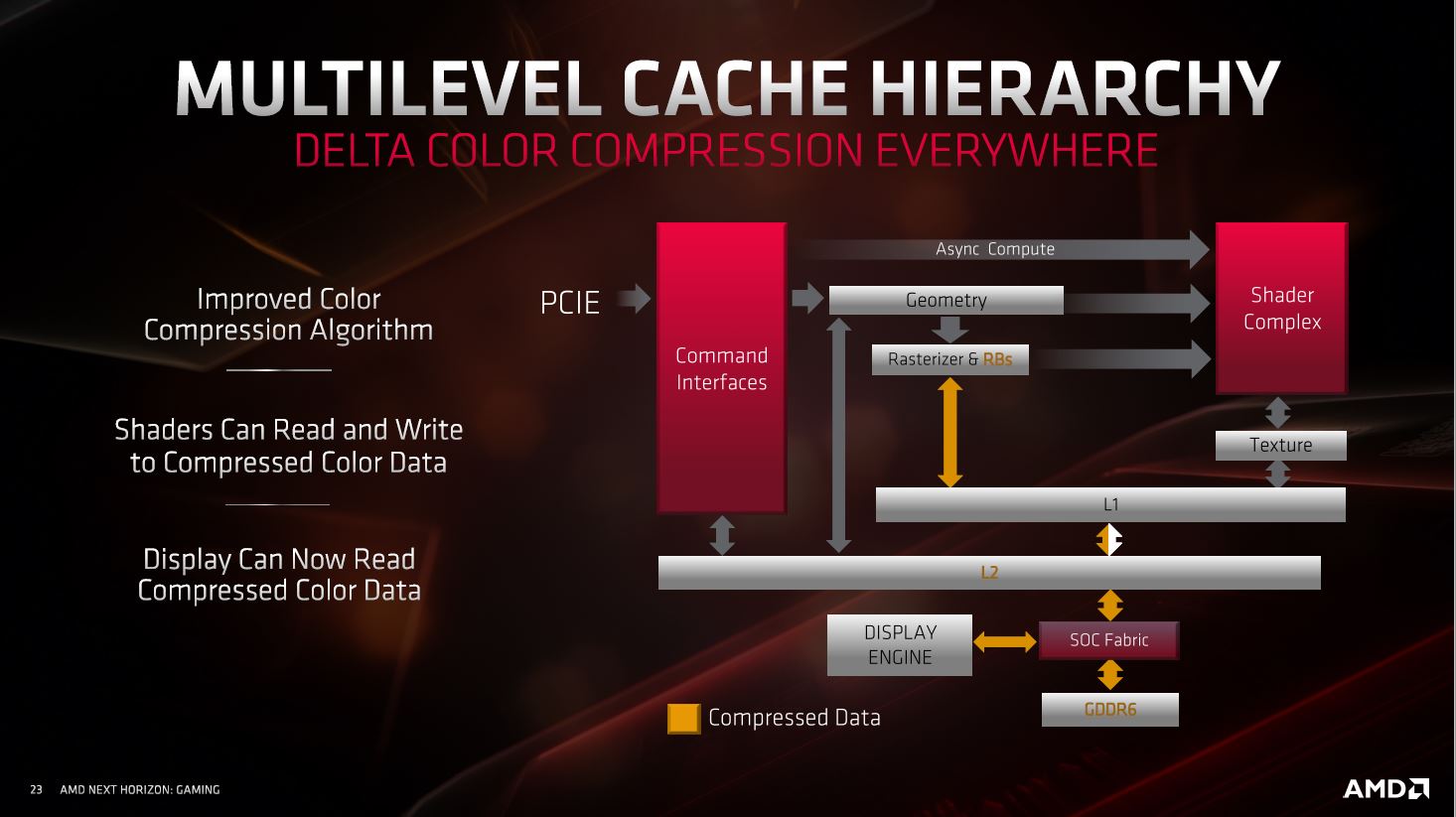
AMD examined previous generations of its graphics architecture to locate bottlenecks in the graphics pipeline. Besides increasing the number of dedicated resources, the company reworked the chip's cache hierarchy by cushioning data transfers at various stages. Each workgroup processor has dedicated 32 KB instruction and 16 KB data caches, which write back to a 128 KB L1 cache dedicated to each Graphics Engine.
These L1 caches talk to 4 MB of L2 cache. The introduction of the L1 cache and doubling in bandwidth between the various caches contributes greatly to IPC as it minimizes memory accesses, which are much slower than cache accesses. AMD is also using faster (lower latency) SRAM that reduces cache latencies by around 20 percent on die and by 8 percent at the memory level. AMD also introduced new features to the ACEs that include async-compute tunneling.

AMD summarizes the benefits of RDNA in a 25 percent IPC gain over the latest version of GCN, and an effective 50 percent performance gain for the GPU when taking into account IPC, the 7 nm process, and gains from the frequency and power management (ability to sustain boost frequencies better).


Elsewhere on the silicon, AMD updated the Display Engine and Multimedia Engine to keep up with the latest display and video standards. The Display Engine now supports DSC 1.2a (display stream compression) along with output standards HDMI 2.0 and DisplayPort 1.4 HDR to support display formats as bandwidth-intensive as 4K 240 Hz or 8K 60 Hz over a single cable, and 30 bits per pixel color depth. The multimedia engine supports VP9 and H.265 decoding at up to 8K 24 Hz, or 4K 90 Hz, and hardware-accelerated H.265 encoding at up to 4K 60 Hz.
Features: FidelityFX and Anti-Lag


With each new graphics architecture, gamers expect new image quality enhancement features. NVIDIA introduced DLSS and AMD's response to that is FidelityFX, a combination of content-specific and image-specific quality enhancements. The first part of this is contrast-adaptive sharpening, which brings out details in a scene by enhancing their contrast. To work best, it requires game developers to declare which parts of the image are to be sharpened (like the HUD and on-screen texts). Details such as wear lines on the slick tires of a race car or hexagonal patterns on a wall come to life. We will test this feature later in a separate article.


AMD wants to improve its adoption by professional e-Sports gamers by addressing a key bottleneck with modern high-end graphics: mouse lag. This would be the amount of time taken for a click to register and a response to be rendered by the GPU. Radeon Anti-Lag is a CTR (click-to-response) enhancement that reduced mouse lag by roughly a third across various popular e-Sports titles. This setting is effectively identical to "pre-rendered" frames on NVIDIA. Modern GPUs calculate one or two frames ahead, so they can better time sending them to the monitor to avoid stuttering. Of course, this results in input lag because any input information that comes in only makes it to the screen one or two frames later.
Packaging and Contents
We received just the card from ASUS without the retail packaging or accessories. Rest assured that the final product will come with proper packaging and bundle.The Card

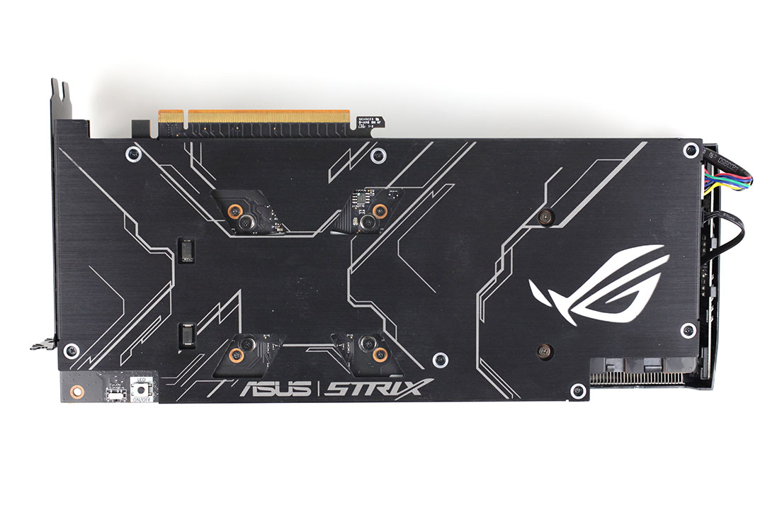
Visually the card looks indistinguishable from the company's GeForce RTX STRIX offers, which is a good thing as it unifies the visual identity of their graphics card. On the back, you'll find a high-quality metal backplate with RGB lighting. Dimensions of the card are 30.0 x 13.5 cm.
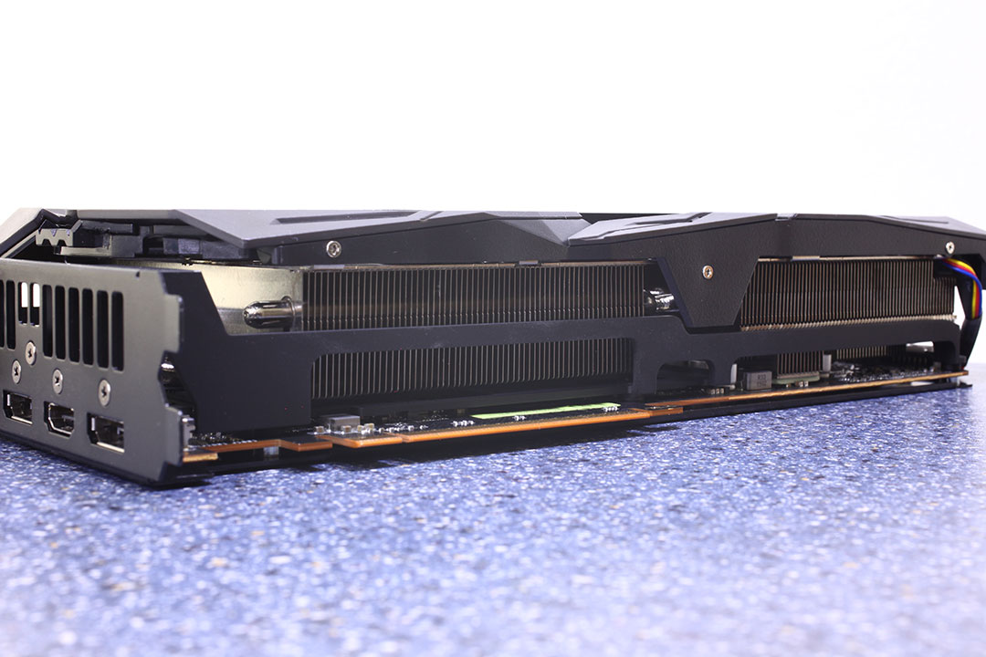
Installation requires three slots in your system.

Display connectivity options include three standard DisplayPort 1.4a and an HDMI 2.0b.
AMD took the opportunity to update the display controllers handling these outputs by leveraging DSC 1.2a (display stream compression), which unlocks very high resolution and refresh-rate combinations over a single cable. Among the single-cable display modes supported are 8K 60 Hz (which took two DP 1.3 cables until now), 4K 240 Hz, and 1080p as high as 360 Hz. On top of these, the outputs support HDR and 30 bpc color-depth for better color accuracy in creative applications.

The board uses two 8-pin power connectors. This input configuration is specified for up to 375 watts of power draw.
AMD's Navi generation of GPUs no longer supports CrossFire. DirectX 12 does include its own set of multi-GPU capabilities, but the implementation requires game developers to put serious development time into a feature only a tiny fraction of their customers might ever use.
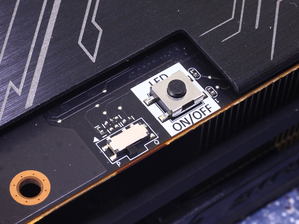
In this area, you'll also find a push button which lets you enable/disable the card's RGB lighting without any software. Right next to that is a dual-BIOS switch with the default setting being "Performance" and the other BIOS "Quiet".
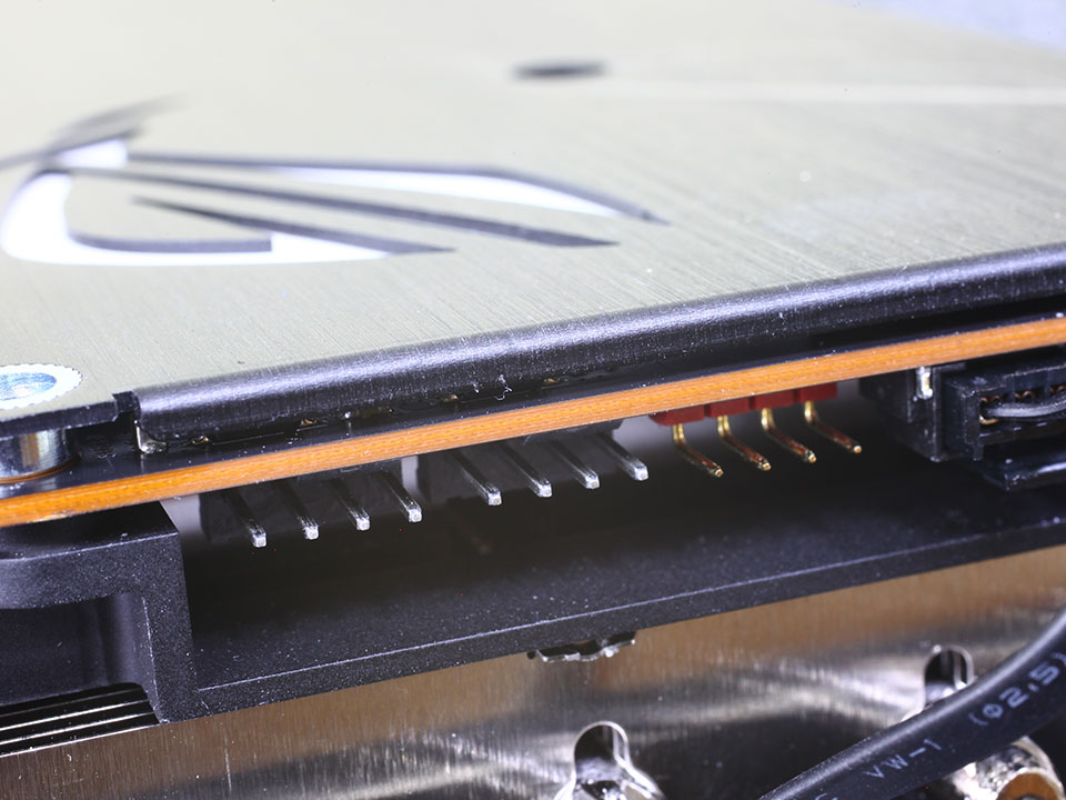
You also get two 4-pin PWM fan headers to sync your case fans to the graphics card's fans and an addressable RGB header other RGB components can be connected to.

After removing the backplate, we found this area, which seems to be good for voltmodders to measure the card's operating voltages easily.
Our Patreon Silver Supporters can read articles in single-page format.
Apr 19th, 2024 01:51 EDT
change timezone
Latest GPU Drivers
New Forum Posts
- Linus watercools (14)
- What's your latest tech purchase? (20283)
- Should the CDPR make the Fallout 5 instead? (23)
- Will a RTX 4070 TI super bottleneck a Ryzen 9 7950X3D? (36)
- DDR5 RAM Speeds and the future (45)
- Cinebench crashed my PC. My Wi-Fi stopped working, and I keep getting a "Please wait" screen when I boot up my PC. (7)
- Adventure: Running 8/9th gen Coffee Lake CPUs on Z170 motherboard (ASUS Maximus VIII Ranger) (336)
- First computer build for my son (1)
- Why is SteamOS taking so long to come to desktop for AMD users, when ChimeraOS is the same thing almost? (19)
- Do you use Linux? (229)
Popular Reviews
- Horizon Forbidden West Performance Benchmark Review - 30 GPUs Tested
- PowerColor Radeon RX 7900 GRE Hellhound Review
- Fractal Design Terra Review
- Corsair 2000D Airflow Review
- Minisforum EliteMini UM780 XTX (AMD Ryzen 7 7840HS) Review
- Thermalright Phantom Spirit 120 EVO Review
- Creative Pebble X Plus Review
- FiiO KB3 HiFi Mechanical Keyboard Review - Integrated DAC/Amp!
- ASUS GeForce RTX 4090 STRIX OC Review
- NVIDIA GeForce RTX 4090 Founders Edition Review - Impressive Performance
Controversial News Posts
- Sony PlayStation 5 Pro Specifications Confirmed, Console Arrives Before Holidays (109)
- NVIDIA Points Intel Raptor Lake CPU Users to Get Help from Intel Amid System Instability Issues (102)
- US Government Wants Nuclear Plants to Offload AI Data Center Expansion (98)
- Windows 10 Security Updates to Cost $61 After 2025, $427 by 2028 (82)
- Developers of Outpost Infinity Siege Recommend Underclocking i9-13900K and i9-14900K for Stability on Machines with RTX 4090 (82)
- TechPowerUp Hiring: Reviewers Wanted for Motherboards, Laptops, Gaming Handhelds and Prebuilt Desktops (71)
- Intel Realizes the Only Way to Save x86 is to Democratize it, Reopens x86 IP Licensing (70)
- AMD Zen 5 Execution Engine Leaked, Features True 512-bit FPU (63)