 44
44
EVGA GeForce GTX 1070 SuperClocked 8 GB Review
(44 Comments) »Introduction
NVIDIA released their GeForce GTX 1070 and GTX 1080 not long ago, featuring the company's new Pascal architecture, a brand-new 16 nanometer production process, and GDDR5X memory. In our launch-day review, we were truly impressed by how well NVIDIA claimed the performance throne with the 1080, but also the GTX 1070 managed to impress with its high-end performance at an attractive sub-$400 price-point. The reference-design card, however, is sold at a $70 premium over the GTX 1070 Founders Edition sitting at $449.
The GeForce GTX 1070 uses the same Pascal GP104 graphics processor as the GTX 1080, with just 1920 enabled shaders instead of 2560, which also affects the number of texture units that are down to 120 from 160. With 64, the number of ROPs is the same, and so is the memory capacity at 8 GB. However, today's review subject, like all GTX 1070 variants, uses GDDR5 memory, unlike the GTX 1080 that comes with GDDR5X. GDDR5X offers twice the bandwidth at the same operating frequency, so NVIDIA is running the GeForce GTX 1070's memory at a frequency of 2 GHz in order to make up for that.

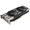
In this review, we're taking a look at the EVGA GTX 1070 SuperClocked, which comes with EVGA's new ACX 3.0 dual-slot, dual-fan thermal solution. Out of the box, the card is clocked at 1595 MHz baseclock; memory remained at the NVIDIA default of 2002 MHz.
The EVGA GTX 1070 SC is currently available online for $439.
| GeForce GTX 970 | Radeon R9 290X | Radeon R9 390X | GeForce GTX 780 Ti | GeForce GTX 980 | Radeon R9 Fury | Radeon R9 Fury X | GeForce GTX 980 Ti | GeForce GTX Titan X | GeForce GTX 1070 | EVGA GTX 1070 SC | GeForce GTX 1080 | |
|---|---|---|---|---|---|---|---|---|---|---|---|---|
| Shader Units | 1664 | 2816 | 2816 | 2880 | 2048 | 3584 | 4096 | 2816 | 3072 | 1920 | 1920 | 2560 |
| ROPs | 56 | 64 | 64 | 48 | 64 | 64 | 64 | 96 | 96 | 64 | 64 | 64 |
| Graphics Processor | GM204 | Hawaii | Hawaii | GK110 | GM204 | Fiji | Fiji | GM200 | GM200 | GP104 | GP104 | GP104 |
| Transistors | 5200M | 6200M | 6200M | 7100M | 5200M | 8900M | 8900M | 8000M | 8000M | 7200M | 7200M | 7200M |
| Memory Size | 4 GB | 4 GB | 8 GB | 3 GB | 4 GB | 4 GB | 4 GB | 6 GB | 12 GB | 8 GB | 8 GB | 8 GB |
| Memory Bus Width | 256 bit | 512 bit | 512 bit | 384 bit | 256 bit | 4096 bit | 4096 bit | 384 bit | 384 bit | 256 bit | 256 bit | 256 bit |
| Core Clock | 1051 MHz+ | 1000 MHz | 1050 MHz | 876 MHz+ | 1126 MHz+ | 1000 MHz | 1050 MHz | 1000 MHz+ | 1000 MHz+ | 1506 MHz+ | 1595 MHz+ | 1607 MHz+ |
| Memory Clock | 1750 MHz | 1250 MHz | 1500 MHz | 1750 MHz | 1750 MHz | 500 MHz | 500 MHz | 1750 MHz | 1750 MHz | 2002 MHz | 2002 MHz | 1251 MHz |
| Price | $265 | $270 | $310 | $390 | $360 | $530 | $600 | $440 | $1150 | $379 / $449 | $439 | $599 / $699 |
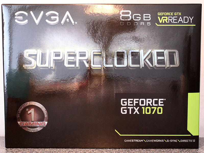
Packaging
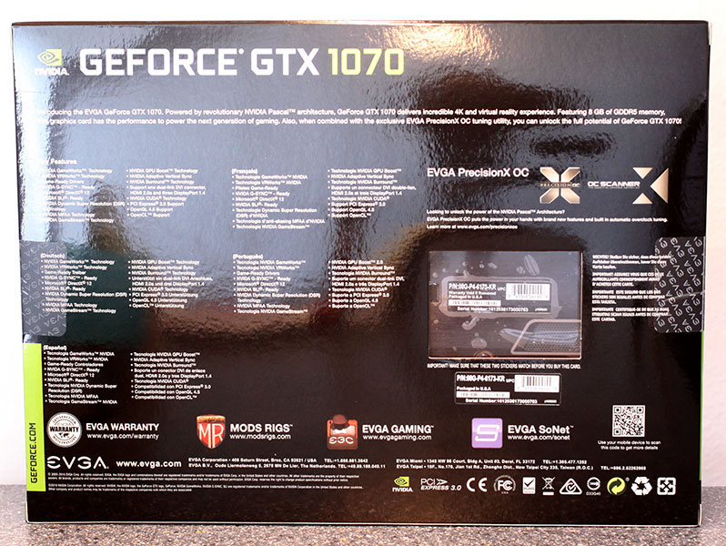
Contents
You will receive:
- Graphics card
- Documentation + EVGA poster
- EVGA case badge
- EVGA stickers
- PCIe power cable
The Card


EVGA's new ACX 3.0 cooler looks mighty good, with large metal surfaces for highlights and black plastic bits to keep cost down. On the back is a high-quality metal backplate with the EVGA logo. Dimensions of the card are 27.0 x 11.5 cm.
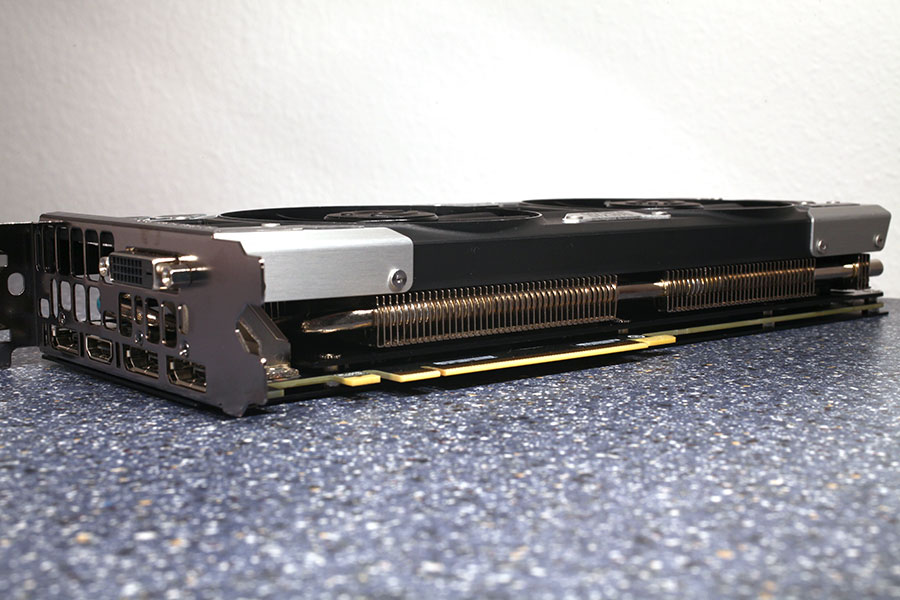
Installation requires two slots in your system.

Display connectivity options include a DVI port, an HDMI port, and three DisplayPorts. Unlike previous NVIDIA cards, the DVI port no longer includes the analog signal, so you'll have to use an active adapter. NVIDIA also updated DisplayPort to be 1.2 certified and 1.3/1.4 ready, which enables support for 4K at 120 Hz and 5K @ 60 Hz, or 8K @ 60 Hz with two cables.
The GPU also comes with an HDMI sound device. It is HDMI 2.0b compatible, which supports HD audio and Blu-ray 3D movies. The GPU video encoding unit has been updated to support HEVC at 10-bit and 12-bit.

NVIDIA made some changes to SLI. Two-way SLI is now the only officially supported configuration for gaming. Three-way or Quad SLI can no longer be enabled in games; however, both do work in a few benchmarks. Also, for 4K at 60 Hz and above, NVIDIA recommends a new high-bandwidth SLI bridge called "SLI HB," which occupies both SLI fingers. The old bridges will work fine at lower resolutions.

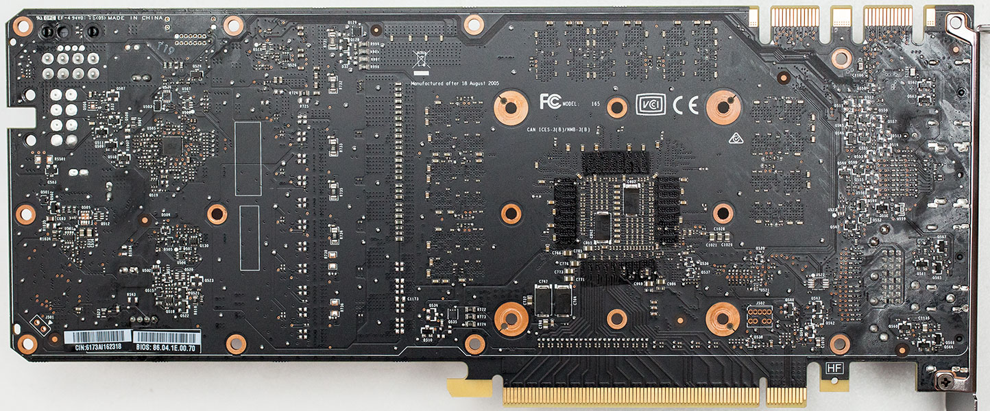
Pictured above are the front and back, showing the disassembled board. High-res versions are also available (front, back).
Our Patreon Silver Supporters can read articles in single-page format.
Jul 29th, 2025 17:08 CDT
change timezone
Latest GPU Drivers
New Forum Posts
- Weird issue with Worms: Armageddon on NV GPUs (8)
- Looking To Make List Of Keyboard Manufacturers (24)
- What's your latest tech purchase? (24392)
- 3D Printer Club (574)
- Dell Workstation Owners Club (3338)
- RX6800XT Gigabyte Gaming OC not giving image while being on "OC" switch and even sometimes while being on "silent" switch. (4)
- 2022-X58/1366 PIN Motherboards NVME M.2 SSD BIOS MOD Collection (949)
- Kindly help me to complete my new PC build... (22)
- Upgrade from old x58 system (57)
- 6400c30 vs 8000c36 Ryzen 9800X3D (39)
Popular Reviews
- Herman Miller Logitech G Embody Review - No Pain, No Gain
- Lian Li O11 Dynamic Mini V2 Review
- Lenovo Legion 5i (15IRX10) Review - Feature-Rich and Wallet Friendly
- MSI Claw 8 AI+ A2VM Review
- Upcoming Hardware Launches 2025 (Updated May 2025)
- Noctua NF-A12x25 G2 PWM Fan Review
- Sapphire Radeon RX 9060 XT Pulse OC 16 GB Review - An Excellent Choice
- AMD Ryzen 7 9800X3D Review - The Best Gaming Processor
- AQIRYS Sirius Pro Review
- VAXEE XE V2 Wireless Review
TPU on YouTube
Controversial News Posts
- AMD's Upcoming UDNA / RDNA 5 GPU Could Feature 96 CUs and 384-bit Memory Bus (134)
- AMD Radeon RX 9070 XT Gains 9% Performance at 1440p with Latest Driver, Beats RTX 5070 Ti (131)
- NVIDIA GeForce RTX 5080 SUPER Could Feature 24 GB Memory, Increased Power Limits (115)
- Intel "Nova Lake-S" Core Ultra 3, Ultra 5, Ultra 7, and Ultra 9 Core Configurations Surface (110)
- DDR6 Memory Arrives in 2027 with 8,800-17,600 MT/s Speeds (100)
- AMD Sampling Next-Gen Ryzen Desktop "Medusa Ridge," Sees Incremental IPC Upgrade, New cIOD (97)
- Intel CEO Confirms SMT To Return to Future CPUs (95)
- NVIDIA Becomes First Company Ever to Hit $4 Trillion Market-Cap (94)