 16
16
Gainward GeForce RTX 4080 Phoenix GS Review
Test Setup »High-resolution PCB Pictures
These pictures are for the convenience of volt modders and people who would like to see all the finer details on the PCB. Feel free to link back to us and use these in your articles, videos or forum posts.

High-resolution versions are also available (front, back).
Circuit Board (PCB) Analysis
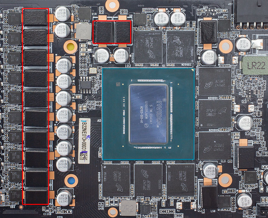

GPU voltage is a 12-phase design, managed by a uPI uP9512R controller.
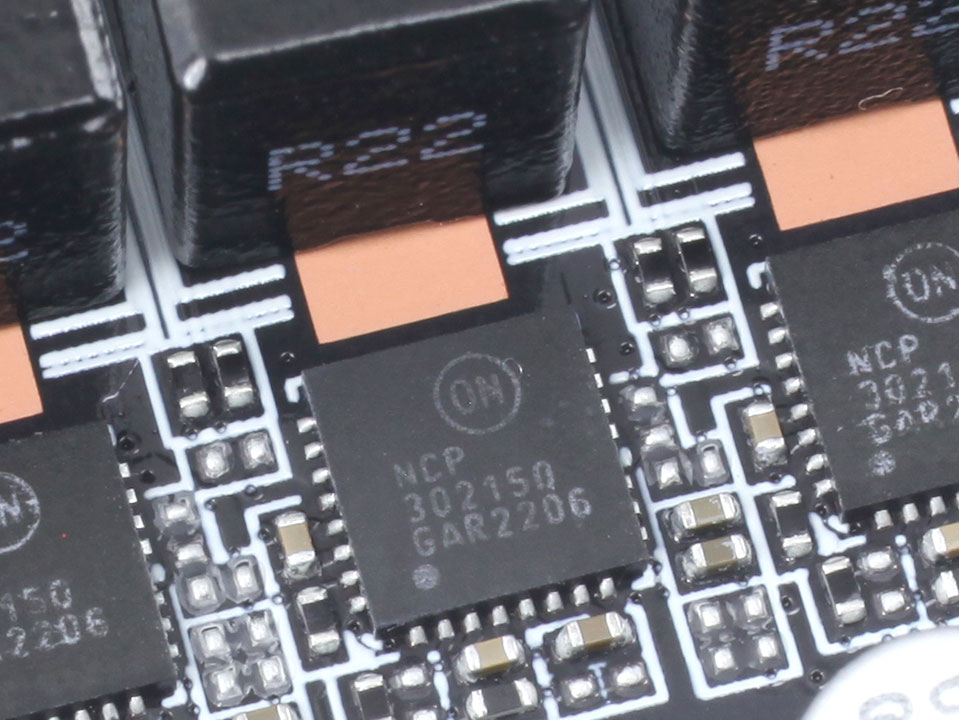
OnSemi NCP302150 DrMOS components are used for GPU voltage; they are rated for 50 A of current each.
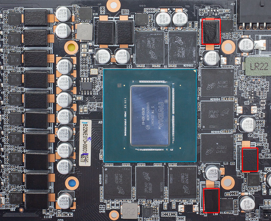

Memory voltage is a three-phase design, managed by a uPI uP9529Q controller.

For memory, OnSemi NCP302150 DrMOS with a 50 A rating are used again.
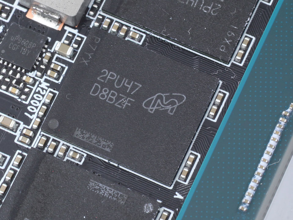
The GDDR6X memory chips are made by Micron and carry the model number D8BZF, which decodes to MT61K512M32KPA-24. They are specified to run at 1500 MHz (24 Gbps effective).

NVIDIA's AD103 graphics processor is the company's second Ada Lovelace GPU. It is built using a 5 nanometer process at TSMC Taiwan, with a transistor count of 45.9 billion and a die size of 379 mm².
Apr 28th, 2024 08:16 EDT
change timezone
Latest GPU Drivers
New Forum Posts
- Which PSU to take? (12)
- XFX RX470 8GB no video and error 43 (31)
- Vintage hardware question! (1)
- problems flashing default bios to dual-bios rx 480 card (7)
- Help me identify rx 580 card ? (4)
- Whats the difference between TUF gaming 4070 ti super oc and non oc? (25)
- rx 6500 xt anisotropic filtering not working (8)
- TPU's Nostalgic Hardware Club (18479)
- DeepCool factory tour - very interesting (4)
- Does a faster NVMe make any difference? (9)
Popular Reviews
- Ugreen NASync DXP4800 Plus Review
- HYTE THICC Q60 240 mm AIO Review
- Upcoming Hardware Launches 2023 (Updated Feb 2024)
- MOONDROP x Crinacle DUSK In-Ear Monitors Review - The Last 5%
- Thermalright Phantom Spirit 120 EVO Review
- FiiO K19 Desktop DAC/Headphone Amplifier Review
- AMD Ryzen 7 7800X3D Review - The Best Gaming CPU
- ASUS Radeon RX 7900 GRE TUF OC Review
- Alienware Pro Wireless Gaming Keyboard Review
- Intel Core i9-14900KS Review - The Last of its Kind
Controversial News Posts
- Windows 11 Now Officially Adware as Microsoft Embeds Ads in the Start Menu (139)
- Sony PlayStation 5 Pro Specifications Confirmed, Console Arrives Before Holidays (117)
- NVIDIA Points Intel Raptor Lake CPU Users to Get Help from Intel Amid System Instability Issues (106)
- AMD "Strix Halo" Zen 5 Mobile Processor Pictured: Chiplet-based, Uses 256-bit LPDDR5X (103)
- US Government Wants Nuclear Plants to Offload AI Data Center Expansion (98)
- AMD's RDNA 4 GPUs Could Stick with 18 Gbps GDDR6 Memory (95)
- Developers of Outpost Infinity Siege Recommend Underclocking i9-13900K and i9-14900K for Stability on Machines with RTX 4090 (85)
- Windows 10 Security Updates to Cost $61 After 2025, $427 by 2028 (84)