 16
16
Gainward GeForce RTX 4080 Phoenix GS Review
(16 Comments) »Introduction
Gainward GeForce RTX 4080 Phoenix GS is the company's affordable custom-design graphics card based on the enthusiast segment "Ada" GPU by NVIDIA. Its name is a callback to the "Golden Sample" (GS) days of Gainward GeForce products from some 20 years ago, and stands for "overclocked" today. Gainward's RTX 4080 lineup includes two distinct product lines, Phantom and Phoenix, with the latter being the flashy, flamboyant product that's loaded with neatly-done RGB LED lighting. We've reviewed the Phantom last year as part of our RTX 4080 launch-day coverage, today we're bringing you the review of the Gainward RTX 4080 Phoenix GS.

The GeForce RTX 4080 is NVIDIA's second fastest graphics card from this generation, and is designed for pretty-much the same class of gamer that goes for the RTX 4090 flagship--to play maxed out at 4K Ultra HD resolution, but at a price that's almost 25% lower, for a $1,200 baseline. You can also max out settings such as real-time ray tracing, and use features such as DLSS 3 frame generation to play at even higher resolutions, such as 5K.
GeForce RTX 4080 is a successor to the RTX 3080 "Ampere," and rocks 16 GB of GDDR6X memory, albeit across a generationally-narrower 256-bit wide memory bus. The new GeForce "Ada" graphics architecture improves the memory sub-system at an architecture level, with significantly larger on-die caches, so the GPU can make do with narrower memory interfaces. The RTX 4080 nearly maxes out the 5 nm AD103 silicon it's based on, with 9.728 CUDA cores, 304 Tensor cores, 76 RT cores, 304 TMUs, and 112 ROPs. It enables 76 out of 80 SM present on the AD103. The 16 GB of GDDR6X memory ticks at 22.4 Gbps, at which it yields 717 GB/s of memory bandwidth.
The Gainward RTX 4080 Phoenix GS in today's review is a factory-overclocked, flashy custom-design graphics card by the company. Despite its RGB bits, the designers tried to keep its cooler shroud surface are to a minimum, exposing more of the meaty aluminium fin-stack heatsink underneath in this big cooler, for better ventilation. The Phoenix GS comes with factory-overclocked speeds of 2610 MHz boost, compared to 2505 MHz reference. With NVIDIA standardizing ATX 12VHPWR with the RTX 40-series, this card features a 16-pin connector that's rated for 600 W power input capability in theory, bundled with an NVIDIA designed adapter that converts three 8-pin connectors to a 16-pin. Gainward is pricing the GeForce RTX 4080 Phoenix GS at 1350 EUR, which converts to USD 1200, so matching NVIDIA reference MSRP.
| Price | Cores | ROPs | Core Clock | Boost Clock | Memory Clock | GPU | Transistors | Memory | |
|---|---|---|---|---|---|---|---|---|---|
| RTX 2080 Ti | $420 | 4352 | 88 | 1350 MHz | 1545 MHz | 1750 MHz | TU102 | 18600M | 11 GB, GDDR6, 352-bit |
| RTX 3070 | $400 | 5888 | 96 | 1500 MHz | 1725 MHz | 1750 MHz | GA104 | 17400M | 8 GB, GDDR6, 256-bit |
| RTX 3070 Ti | $520 | 6144 | 96 | 1575 MHz | 1770 MHz | 1188 MHz | GA104 | 17400M | 8 GB, GDDR6X, 256-bit |
| RX 6800 | $480 | 3840 | 96 | 1815 MHz | 2105 MHz | 2000 MHz | Navi 21 | 26800M | 16 GB, GDDR6, 256-bit |
| RX 6800 XT | $560 | 4608 | 128 | 2015 MHz | 2250 MHz | 2000 MHz | Navi 21 | 26800M | 16 GB, GDDR6, 256-bit |
| RTX 3080 | $570 | 8704 | 96 | 1440 MHz | 1710 MHz | 1188 MHz | GA102 | 28000M | 10 GB, GDDR6X, 320-bit |
| RTX 3080 Ti | $750 | 10240 | 112 | 1365 MHz | 1665 MHz | 1188 MHz | GA102 | 28000M | 12 GB, GDDR6X, 384-bit |
| RX 6900 XT | $680 | 5120 | 128 | 2015 MHz | 2250 MHz | 2000 MHz | Navi 21 | 26800M | 16 GB, GDDR6, 256-bit |
| RX 6950 XT | $800 | 5120 | 128 | 2100 MHz | 2310 MHz | 2250 MHz | Navi 21 | 26800M | 16 GB, GDDR6, 256-bit |
| RTX 3090 | $850 | 10496 | 112 | 1395 MHz | 1695 MHz | 1219 MHz | GA102 | 28000M | 24 GB, GDDR6X, 384-bit |
| RTX 4070 Ti | $820 | 7680 | 80 | 2310 MHz | 2610 MHz | 1313 MHz | AD104 | 35800M | 12 GB, GDDR6X, 192-bit |
| RX 7900 XT | $880 | 5376 | 192 | 2000 MHz | 2400 MHz | 2500 MHz | Navi 31 | 57700M | 20 GB, GDDR6, 320-bit |
| RTX 3090 Ti | $1400 | 10752 | 112 | 1560 MHz | 1950 MHz | 1313 MHz | GA102 | 28000M | 24 GB, GDDR6X, 384-bit |
| RTX 4080 | $1200 | 9728 | 112 | 2205 MHz | 2505 MHz | 1400 MHz | AD103 | 45900M | 16 GB, GDDR6X, 256-bit |
| Gainward RTX 4080 Phoenix GS | $1200 | 9728 | 112 | 2205 MHz | 2610 MHz | 1400 MHz | AD103 | 45900M | 16 GB, GDDR6X, 256-bit |
| RX 7900 XTX | $1000 | 6144 | 192 | 2300 MHz | 2500 MHz | 2500 MHz | Navi 31 | 57700M | 24 GB, GDDR6, 384-bit |
| RTX 4090 | $1600 | 16384 | 176 | 2235 MHz | 2520 MHz | 1313 MHz | AD102 | 76300M | 24 GB, GDDR6X, 384-bit |
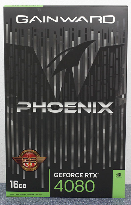
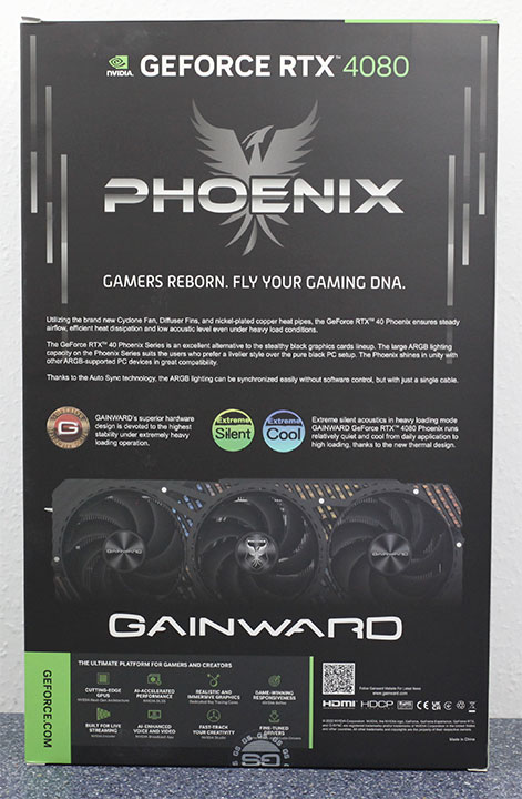
Packaging
The Card


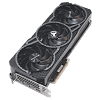
Gainward's cards comes with a complex industrial look on the main cooler, maybe reminding me a bit of alien structures in sci-fi movies. On the back you get a high-quality metal backplate, the front cooler shroud is made from plastic.

Gainward has integrated an RGB lighting element along the top edge and there's more lighting around the fans.


Dimensions of the card are 33.0 x 13.0 cm, and it weighs 1591 g.


Installation requires three slots in your system. Actually the card is 3.1 slots, so you should be able to fix a card right next to it if it's something small without a backplate.

Display connectivity includes three standard DisplayPort 1.4a ports and one HDMI 2.1a (same as Ampere).
NVIDIA introduced the concept of dual NVDEC and NVENC Codecs with the Ada Lovelace architecture. This means there are two independent sets of hardware-accelerators; so you can encode and decode two streams of video in parallel or one stream at double the FPS rate. The new 8th Gen NVENC now accelerates AV1 encoding, besides HEVC. You also get an "optical flow accelerator" unit that is able to calculate intermediate frames for videos, to smooth playback. The same hardware unit is used for frame generation in DLSS 3.

The card uses the new 12+4 pin ATX 12VHPWR connector, which is rated for up to 600 W of power draw. An adapter cable from 3x PCIe 8-pin is included (which is rated for up to 450 W). Of course the 4x 8-pin to 16-pin adapter cables from RTX 4090 will also work with the RTX 4080, but the card won't need that much power.
Right next to the power connector you find the ARGB header, which lets you sync the graphics card's lighting effects with the rest of your system.
Teardown


The cooler on the Phoenix GS uses eight heatpipes that move heat away quickly from the GPU surface. The main cooler also provides cooling for the VRM and memory chips.


The backplate is made of metal and protects the card against damage during installation and handling.
High-resolution PCB Pictures
These pictures are for the convenience of volt modders and people who would like to see all the finer details on the PCB. Feel free to link back to us and use these in your articles, videos or forum posts.

High-resolution versions are also available (front, back).
Circuit Board (PCB) Analysis
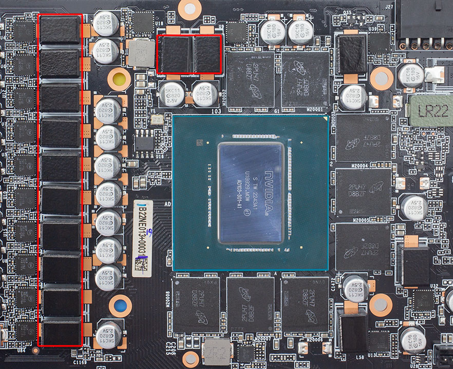

GPU voltage is a 12-phase design, managed by a uPI uP9512R controller.
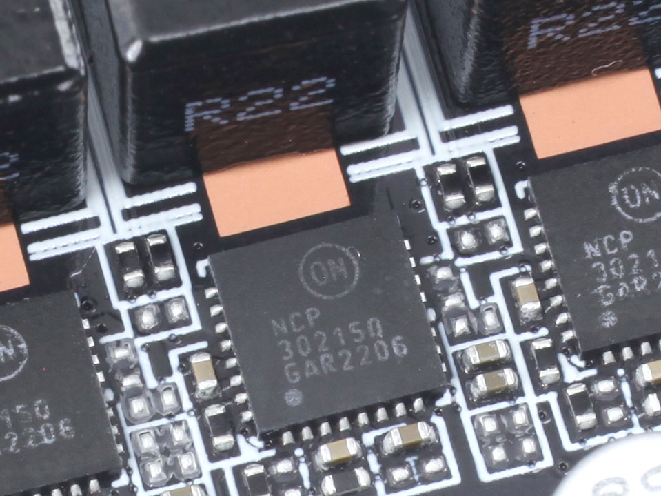
OnSemi NCP302150 DrMOS components are used for GPU voltage; they are rated for 50 A of current each.
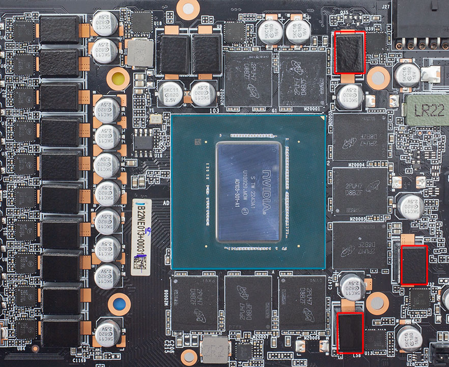

Memory voltage is a three-phase design, managed by a uPI uP9529Q controller.

For memory, OnSemi NCP302150 DrMOS with a 50 A rating are used again.
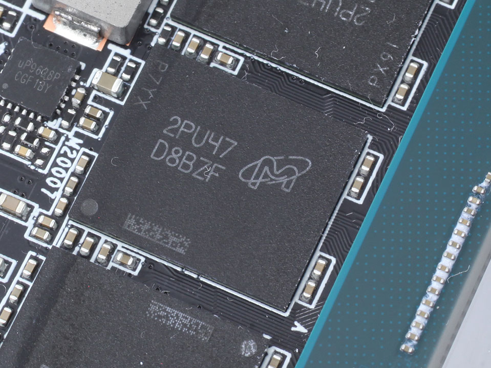
The GDDR6X memory chips are made by Micron and carry the model number D8BZF, which decodes to MT61K512M32KPA-24. They are specified to run at 1500 MHz (24 Gbps effective).

NVIDIA's AD103 graphics processor is the company's second Ada Lovelace GPU. It is built using a 5 nanometer process at TSMC Taiwan, with a transistor count of 45.9 billion and a die size of 379 mm².
Test System
| Test System - GPU 2023.1 | |
|---|---|
| Processor: | Intel Core i9-13900K (Raptor Lake, 36 MB Cache) PL1 = PL2 = 320 W |
| Motherboard: | EVGA Z790 Dark BIOS 1.10 |
| Resizable BAR: | Enabled on all supported AMD, NVIDIA & Intel cards |
| Memory: | Thermaltake TOUGHRAM, 2x 16 GB DDR5-6000 MHz 36-38-38-76 |
| Cooling: | Arctic Liquid Freezer II 280 mm AIO |
| Thermal Paste: | Arctic MX-6 |
| Storage: | 2x Neo Forza NFP455 2 TB M.2 NVMe SSD |
| Power Supply: | Seasonic Vertex GX 850 W ATX 3.0 |
| Case: | darkFlash DLX4000 Mesh |
| Operating System: | Windows 11 Professional 64-bit Version 22H2 |
| Drivers: | NVIDIA: 528.02 WHQL RX 7900 XT & XTX: 23.1.2 Beta AMD: 22.11.2 WHQL |


- All games and cards are tested with the drivers listed above—no performance results were recycled between test systems. Only this exact system with exactly the same configuration is used.
- All graphics cards are tested using the same game version.
- All games are set to their highest quality setting unless indicated otherwise.
- AA and AF are applied via in-game settings, not via the driver's control panel.
- Before starting measurements, we heat up the card for each test to ensure a steady state is tested. This ensures that the card won't boost to unrealistically high clocks for only a few seconds until it heats up, as that doesn't represent prolonged gameplay.
- For better real-life applicability, all game tests use custom in-game test scenes, not the integrated benchmarks
- All cards used for comparison are reference designs. When a reference design does not exist, we go the extra mile and buy the closest possible match, using reference clocks and default power limit.
- 1920x1080: Most popular monitor resolution.
- 2560x1440: Intermediary resolution between Full HD and 4K, with reasonable performance requirements.
- 3840x2160: 4K Ultra HD resolution, available on the latest high-end monitors.
Our Patreon Silver Supporters can read articles in single-page format.
Jul 30th, 2025 05:16 CDT
change timezone
Latest GPU Drivers
New Forum Posts
- Slow textures problems and Pop in objects on new system. RTX 5080 (32)
- AMD Radeon 6900 XT Limited Black Edition Bios Problems - Boost Problems (1)
- What antivirus do you use? (52)
- LCD IPS display (12)
- What's your latest tech purchase? (24397)
- AI Job Losses: let's count the losses up, total losses to AI so far 94,000 and counting (80)
- I stop using Windows as my main OS for like 4+ years (7)
- 3DMARK "LEGENDARY" (346)
- ASUS ROG Strix B850-I Gaming Wi-Fi (5)
- 5070ti or 9070xt? (66)
Popular Reviews
- Herman Miller Logitech G Embody Review - No Pain, No Gain
- MSI Claw 8 AI+ A2VM Review
- Lenovo Legion 5i (15IRX10) Review - Feature-Rich and Wallet Friendly
- Lian Li O11 Dynamic Mini V2 Review
- Upcoming Hardware Launches 2025 (Updated May 2025)
- Noctua NF-A12x25 G2 PWM Fan Review
- Sapphire Radeon RX 9060 XT Pulse OC 16 GB Review - An Excellent Choice
- AMD Ryzen 7 9800X3D Review - The Best Gaming Processor
- AQIRYS Sirius Pro Review
- NVIDIA GeForce RTX 5050 8 GB Review
TPU on YouTube
Controversial News Posts
- AMD's Upcoming UDNA / RDNA 5 GPU Could Feature 96 CUs and 384-bit Memory Bus (134)
- AMD Radeon RX 9070 XT Gains 9% Performance at 1440p with Latest Driver, Beats RTX 5070 Ti (131)
- Intel "Nova Lake-S" Core Ultra 3, Ultra 5, Ultra 7, and Ultra 9 Core Configurations Surface (110)
- DDR6 Memory Arrives in 2027 with 8,800-17,600 MT/s Speeds (101)
- AMD Sampling Next-Gen Ryzen Desktop "Medusa Ridge," Sees Incremental IPC Upgrade, New cIOD (97)
- Intel CEO Confirms SMT To Return to Future CPUs (95)
- NVIDIA Becomes First Company Ever to Hit $4 Trillion Market-Cap (94)
- Windows 12 Delayed as Microsoft Prepares Windows 11 25H2 Update (92)