 187
NVIDIA GeForce RTX 5050 8 GB Review
Test Setup »High-resolution PCB Pictures
These pictures are for the convenience of volt modders and people who would like to see all the finer details on the PCB. Feel free to link back to us and use these in your articles, videos or forum posts.

High-resolution versions are also available (front, back).
Circuit Board (PCB) Analysis
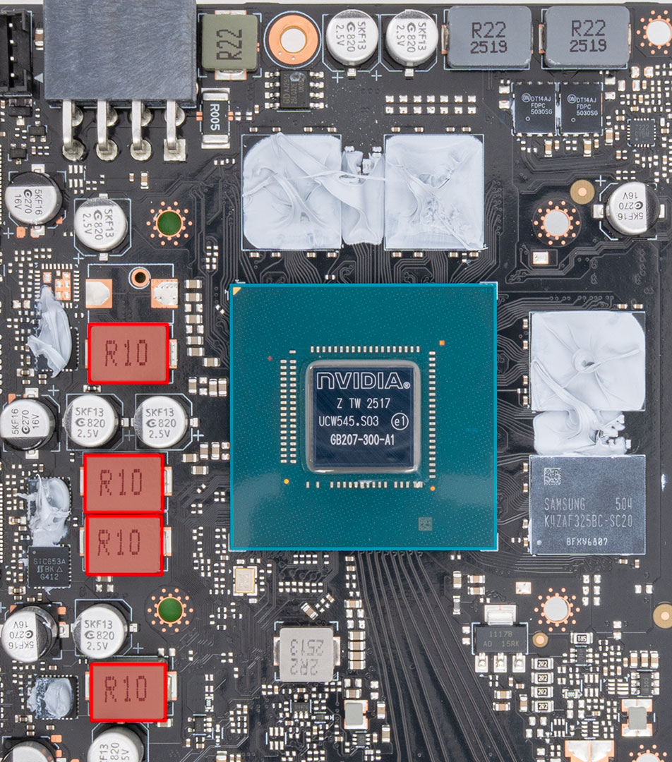

A 4-phase VRM powers the GPU, highlighted in the red rectangles above. These are controlled by an Alpha & Omega AOZ73004CQI (ENC0) voltage controller.
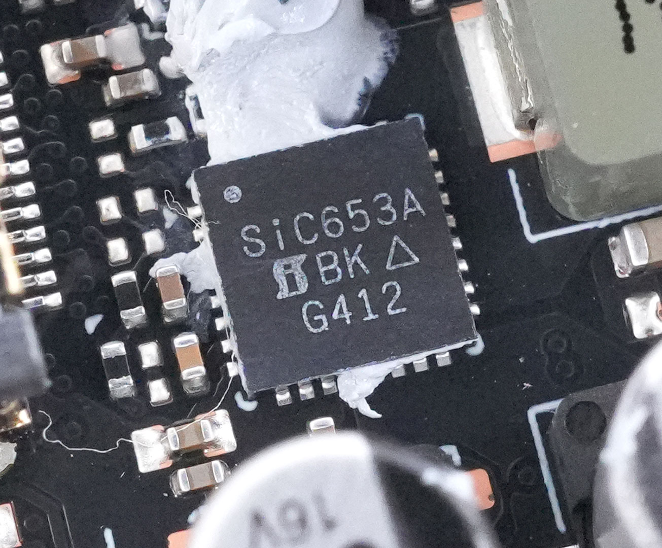
The GPU VRM uses Vishay SIC653A DrMOS components rated for 50 A.
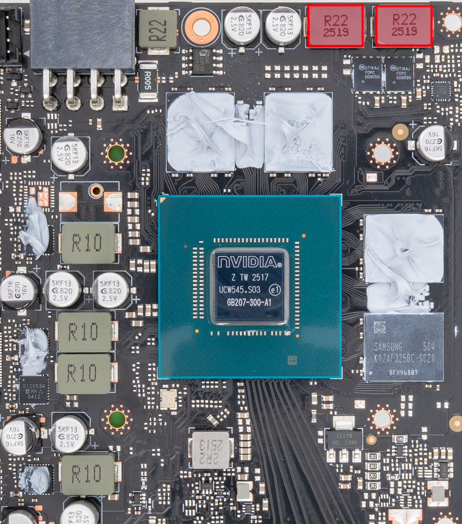
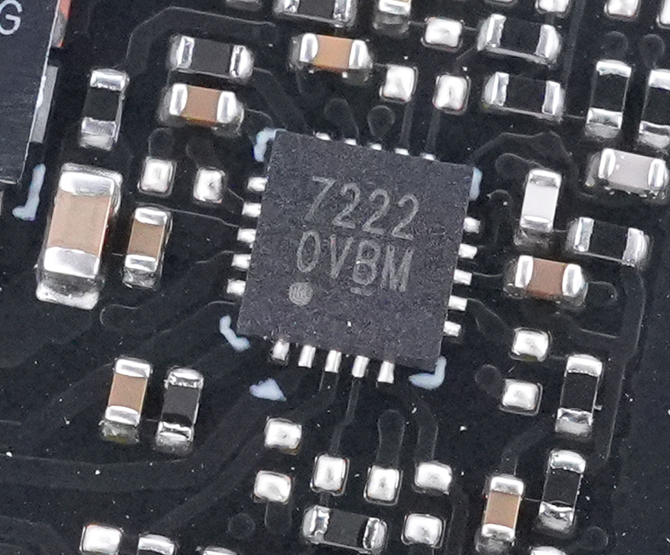
Powering the four GDDR6 memory chips is a 2-phase VRM driven by a 7222 buck controller.

For memory, OnSemi FDPC5030SG dual MOSFETs are used with a 25 A rating.
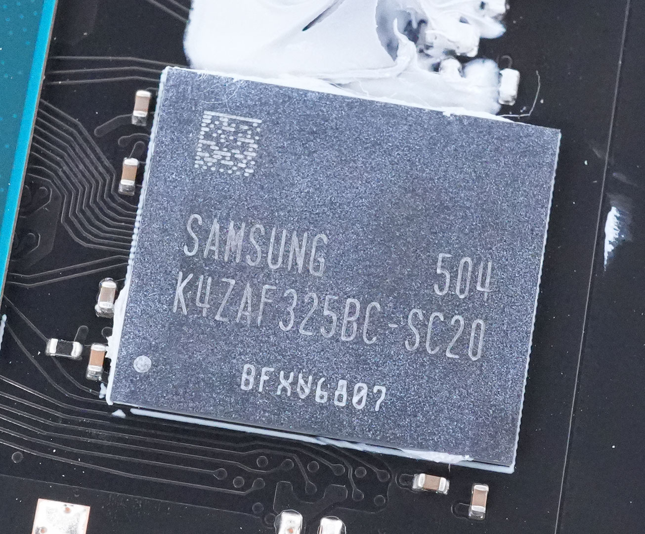
The GDDR6 memory chips are made by Samsung, and bear the model number K4ZAF325BC-SC20, they are rated for 20 Gbps.

The NVIDIA GB207 GPU at the heart of the GeForce RTX 5050—this is a different GPU than on the RTX 5060 Series. It is fabricated using a 5 nanometer "NVIDIA 4N" process at TSMC Taiwan (same process as Ada). We measured the die size to be around 149 mm². NVIDIA confirmed a transistor count of 16.9 billion.
Nov 15th, 2026 01:54 CST
change timezone
Latest GPU Drivers
New Forum Posts
- Honestly, do you care about GTA VI? (39)
- Optical Disc Drive owners club (210)
- WarpCoreBench scores! (46)
- Bought MAX-P495 - Which model? (32)
- "Legacy Control Panel" won't install (1)
- Tell me about your favourite graphics card (84)
- Planning for Prolonged High Prices and Maintaining What You Already Have (72)
- What can the FX 8320 do today? Here is the answer. (47)
- Recommendations Wanted - Affordable Enterprise SSD for Boot (3)
- [INTEL]-How To Update Your Microcode for Intel HX 13/14th Gen. CPUs Laptops/Mobile Easily. (260)
Popular Reviews
- AMD Zen 6 Technical Deep Dive
- ASUS ROG Strix B850-I Gaming Wi-Fi7 W Review
- Corsair HX1000i Shift Crystal Review
- Upcoming Hardware Launches 2027 (Updated Nov 2026)
- Montech King 95 3D PRO Review
- NZXT C1200 Platinum Review
- NZXT H7 RGB+ Review
- NZXT H5 Review
- Phantom Blade Zero Performance Benchmark Review - 35 GPUs Tested
- AMD Ryzen 7 9800X3D Review - The Best Gaming Processor
TPU on YouTube
Controversial News Posts
- NVIDIA Co-Founder and CEO Jensen Huang Officially Resigns (408)
- OpenAI CEO Argues Home PCs Waste the World's Limited DRAM Supply (152)
- NVIDIA Launches Investigation Into Jensen Huang's Relationship With Suspected Chinese Spy (136)
- Intel "Raptor Lake Next" 16-Core and 20-Core CPUs Surface (130)
- Legendary Game Studio BioWare Shuts Down Following EA Layoffs (104)
- Dell CEO Says the Memory Shortage Will Get Worse in 2027 (95)
- NVIDIA GeForce RTX 50-Series Scheduled for up to $500 Price Hike This Week (89)
- Modder Fits RTX 5090 With Four 8-Pin Connectors, Halving Current per Wire (80)