 126
Intel Panther Lake Technical Deep Dive
(126 Comments) »Introduction

We were invited to Intel's Tech Tour 2025 event in Arizona—the site of the brand-new Intel 18A fab—to see how the company plans to deliver its next mobile platform, Panther Lake. The visit provided plenty of briefings (the full slide decks are on the last page), but also rare, on-and off-the-record access to key people, engineers, etc. This helped us connect process technology, packaging, and architecture into a single story. This article distills those briefings and demos into a clear look at what's new, why it matters, and where Panther Lake fits.

While the 18A process is the foundation for it, Panther Lake is more than just a new manufacturing node—it's a complete platform overhaul. Besides the new process, it uses RibbonFET transistors and PowerVia backside power delivery in an architecture that combines new Cougar Cove P-cores, Darkmont E-cores, and low-power cores, all managed by a smarter Thread Director. A faster next-generation fabric links the CPU, GPU, NPU, and IPU, allowing them to share data smoothly and efficiently. The new Xe3 graphics architecture greatly improves performance, adds multi-frame generation, and works closely with the NPU and IPU for AI and media tasks. With Foveros-S packaging, Wi-Fi 7, and improved power control, Panther Lake should be able to deliver higher performance, better sustained performance, improved efficiency, and faster responsiveness across all types of workloads.
What follows is a practical tour of the platform: process and packaging advances, the product stack and tile configurations, CPU and cache changes, the updated fabric, scheduling and power management, Xe3 integrated graphics, connectivity, and the AI/media engines. We'll also summarize Intel's performance claims and timelines to set expectations ahead of launch. If Panther Lake delivers on these fundamentals, it could mark a big step forward for Intel's mobile lineup.
Process and Packaging Innovations

Intel 18A is the most advanced process technology the company has brought into mass production so far. The "18A" designation refers to a feature size in the 1.8-nanometer class, meaning the transistors and wiring are smaller and more tightly packed than before. Shrinking these structures increases transistor density and reduces switching energy, allowing higher performance within the same power and thermal limits. For notebook chips such as Panther Lake, this enables better efficiency without a noticeable increase in heat or battery use. Intel indicates gate lengths are roughly 5–10% shorter moving from FinFET to RibbonFET on 18A, with a >20% per-transistor power reduction.


Intel 18A introduces the RibbonFET transistor, Intel's implementation of a gate-all-around design. Instead of the vertical fins used in FinFET technology, several thin horizontal ribbons of silicon are surrounded on all sides by the control gate. This gives tighter electrical control and allows lower operating voltages. RibbonFET is not unique to Intel—foundries such as TSMC and Samsung have also moved to gate-all-around structures in their latest process nodes—but 18A is Intel's first large-scale deployment of the concept.
In cross-section, each ribbon acts as an individual channel completely wrapped by the gate material. This geometry reduces leakage current and improves efficiency when the transistor switches. Intel combines this structure with improved materials and shorter gate lengths to sustain high performance, while continuing to reduce power draw.


The second major change in Intel 18A is PowerVia, a backside power delivery system. Traditional chips route both data and power through the same top metal layers, leading to congestion and voltage loss. PowerVia moves the power network to the reverse side of the wafer, freeing the front for data signals. This shortens the distance between transistors and their power sources, reducing resistance and helping maintain stable voltages at high switching speeds.
Separating power and signal routing improves both energy efficiency and circuit layout flexibility. Intel's internal data shows lower power loss and better frequency scaling compared with earlier nodes. PowerVia complements RibbonFET: one focuses on transistor control, the other on delivering clean power to each device.
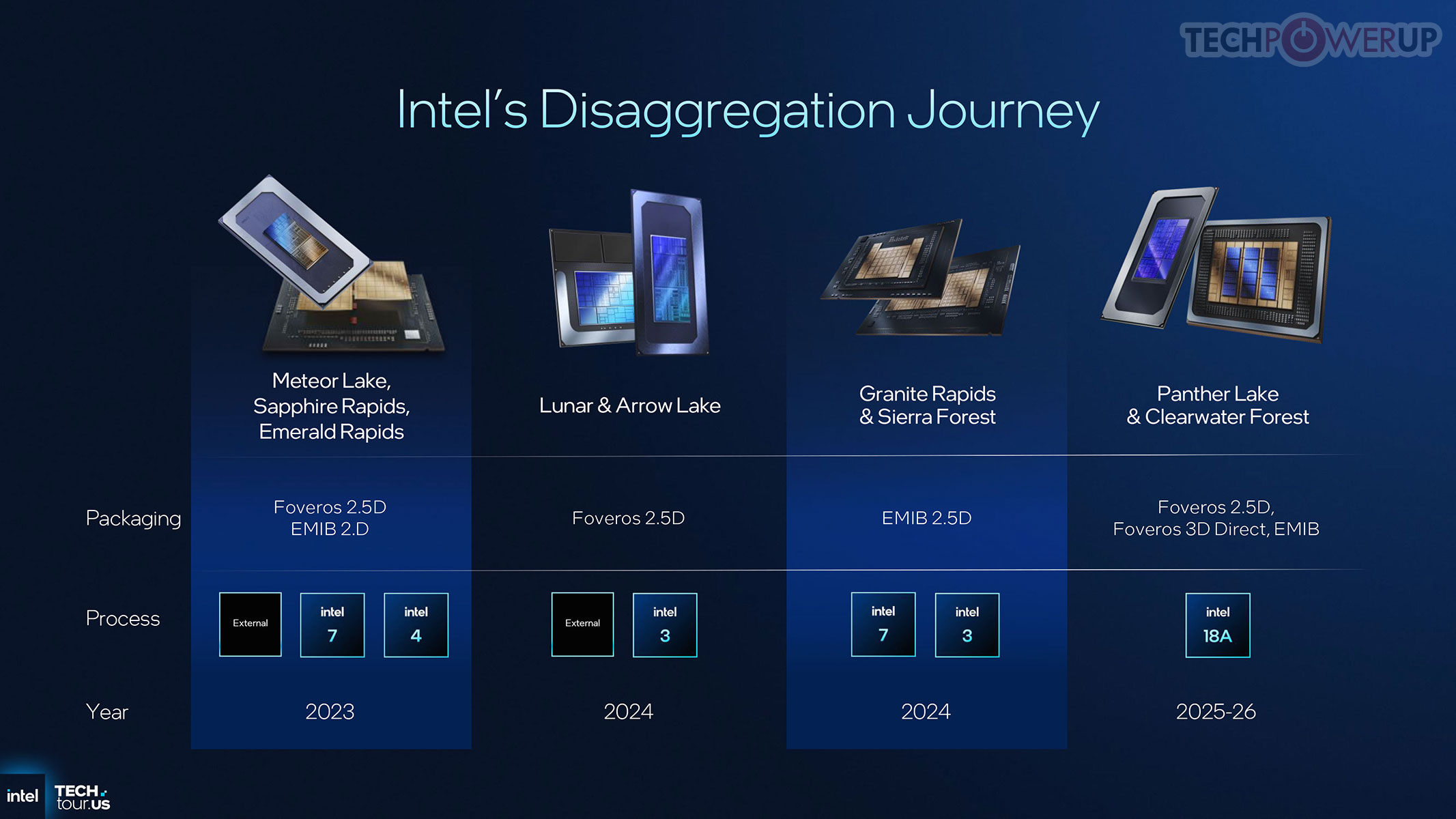
At the chip-assembly level, Intel uses Foveros packaging to connect multiple smaller dies, or tiles, into a single product. Instead of a single large monolithic die, several specialized tiles are linked either vertically (3D) or side-by-side on a thin silicon base (2.5D). This modular construction improves yields and allows each tile to use the most appropriate process node. Intel is not alone in this approach; AMD's Ryzen and EPYC processors were early examples of using multiple chiplets connected by an internal fabric, proving the model can scale efficiently.
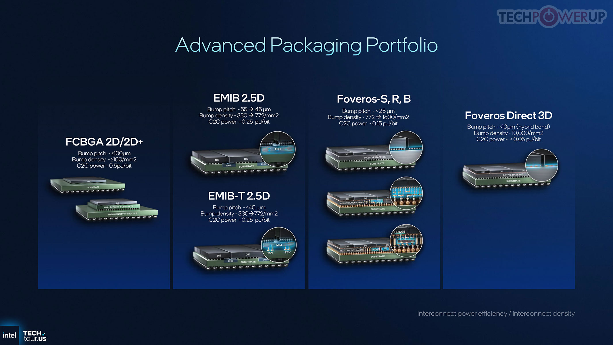
Panther Lake employs Foveros-S, a 2.5D version with fine-pitch interconnects of 36 micrometers. It links compute, graphics, and platform controller tiles into a cohesive SoC. Foveros is Intel's in-house implementation of a broader industry shift toward multi-die packaging, which now includes competing technologies such as AMD's Infinity Fabric, TSMC's CoWoS, and Samsung's I-Cube. These packaging methods have collectively reshaped chip production by allowing companies to mix different process nodes and IP blocks in one package. Processes used: the compute tile is Intel 18A; the 12-Xe GPU tile uses TSMC N3E; the 4-Xe GPU tile is on Intel 3; and the platform controller (PCH) tile is on TSMC N6—joined using Foveros-S 2.5D. Using different nodes per tile is part of Intel's IDM 2.0 flexibility to meet timing/yield/performance goals.
The combination of smaller transistors, cleaner power delivery, and modular packaging forms the foundation of the Panther Lake platform. Intel 18A, RibbonFET, PowerVia, and Foveros together allow Intel to build processors that are more efficient, more flexible, and easier to adapt across product lines—this is part of a wider industry movement toward disaggregated system-on-chip design rather than unique, monolithic dies for each generation, which are expensive to make, and due to their large size are prone to defects, reducing yield rates.
Panther Lake in Intel's Lineup


The roadmap slide outlines Intel's recent mobile client CPU progression from Meteor Lake through Lunar Lake and Arrow Lake, to Panther Lake. Meteor Lake introduced the first disaggregated, tile-based client SoC, Lunar Lake pushed that model toward lower power and integrated memory, and Arrow Lake focused on higher performance with larger tiles. Panther Lake takes the next step by combining both efficiency- and performance-oriented cores into a single design that is able to scale across multiple notebook segments.

Intel Panther Lake is the company's first processor to use its new Intel 18A process for the compute tile with GPU tiles built on Intel 3 or TSMC N3E, all paired with externally manufactured tiles produced by TSMC. This mix of in-house and external manufacturing marks a shift toward a hybrid supply strategy where Intel Foundry Services focuses on core logic, while other tiles continue to come from outside partners.

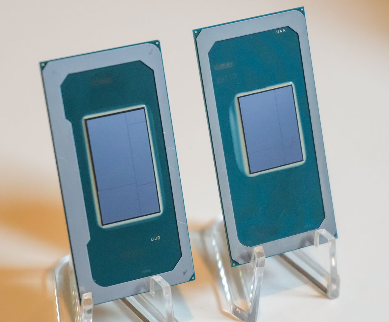
Above, we have a photo of an Intel 18A wafer for Panther Lake that I took at the event, and next to it, two Panther Lake configurations—you can see the individual tiles very well.

Panther Lake is available in three configurations, consisting of a mix of various dies, but all following the same underlying combination approach. Each Panther Lake SoC consists of a compute tile, GPU tile, and platform controller tile connected through Intel's second-generation scalable fabric. This approach allows Intel to reuse building blocks while varying configurations for different product targets.


Panther Lake sits between Lunar Lake and Arrow Lake in both performance and power range. It extends the efficiency characteristics of Lunar Lake into higher-performance systems and overlaps with Arrow Lake in the mainstream notebook space. Intel did not clarify what happens to Arrow Lake mobile once Panther Lake launches. It remains unclear whether both product lines will coexist or whether Panther Lake will completely replace Arrow Lake in Intel's laptop lineup.
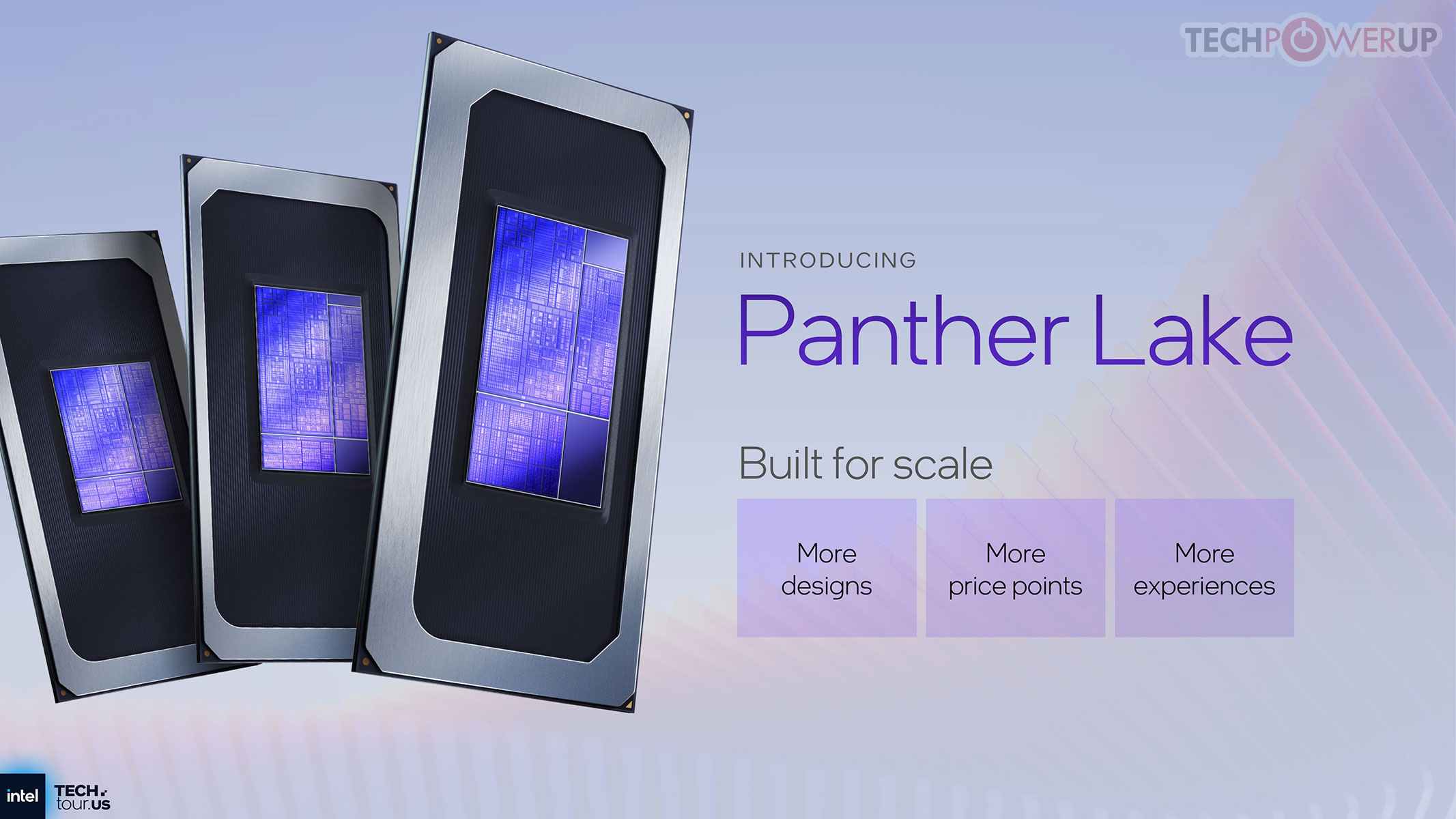
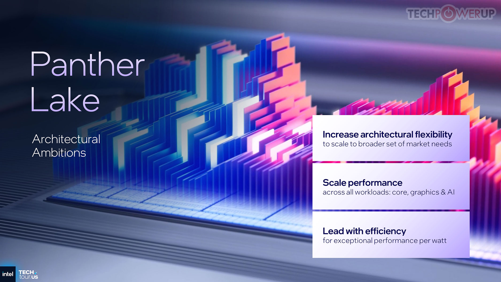
Intel's messaging frames Panther Lake as the architecture that unifies its mobile portfolio under one design. The platform follows three guiding principles: improve performance per watt, scale compute and graphics performance across a wide power range, and increase configurability. No desktop variant was mentioned during the presentations, suggesting that Panther Lake will remain a mobile-only platform. For now, it represents Intel's effort to merge efficiency-focused and performance-focused client products into a single scalable roadmap centered on notebook platforms.
Our Patreon Silver Supporters can read articles in single-page format.
Nov 12th, 2026 11:12 PST
change timezone
New Forum Posts
- When you could finally run Crysis maxed out? (50)
- TPU's Nostalgic Hardware Club (22148)
- 3050 Ti 120W TGP Shunt Mod Result [Legion 5 2021] (5)
- I won't download games that are larger than 30–40 GB. (89)
- Any other old-timers here planning to play WoW Forever? (148)
- So I fixed the r36s “k36” variant and clone with an Onn 128gb sd card and the Onn sd card reader and it BOOTED..so real neat! Take a look. (3)
- Windows 11 General Discussion (7724)
- I forced a 16 Year Old 64GB SSD to write 1 PETABYTE (And it didn't die) (192)
- The TPU Darkroom - Digital SLR and Photography Club (4494)
- WarpCoreBench scores! (15)
Popular Reviews
- AMD Zen 6 Technical Deep Dive
- Upcoming Hardware Launches 2027 (Updated Nov 2026)
- NZXT C1200 Platinum Review
- XPG NIMBUS PLUS Review - Mid-range Chair With Strong Competitors
- NZXT H7 RGB+ Review
- Montech King 95 3D PRO Review
- NZXT H5 Review
- Phantom Blade Zero Performance Benchmark Review - 35 GPUs Tested
- Corsair HX1000i Shift Crystal Review
- Gigabyte Z890I Aorus Ultra Review
TPU on YouTube
Controversial News Posts
- NVIDIA Co-Founder and CEO Jensen Huang Officially Resigns (201)
- OpenAI CEO Argues Home PCs Waste the World's Limited DRAM Supply (152)
- NVIDIA Launches Investigation Into Jensen Huang's Relationship With Suspected Chinese Spy (136)
- Intel "Raptor Lake Next" 16-Core and 20-Core CPUs Surface (130)
- Legendary Game Studio BioWare Shuts Down Following EA Layoffs (104)
- Dell CEO Says the Memory Shortage Will Get Worse in 2027 (95)
- NVIDIA GeForce RTX 50-Series Scheduled for up to $500 Price Hike This Week (89)
- Modder Fits RTX 5090 With Four 8-Pin Connectors, Halving Current per Wire (80)