 15
15
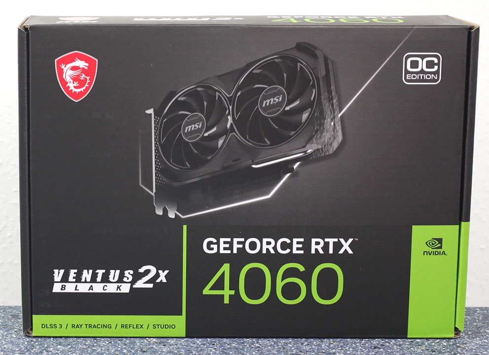
MSI GeForce RTX 4060 Ventus 2X OC Review
(15 Comments) »Introduction
MSI GeForce RTX 4060 Ventus 2X is the company's most affordable custom-design rendition of NVIDIA's latest mid-range graphics card. The new GeForce RTX 4060 is designed for 1080p gaming with maxed out settings. Positioned a notch below the recently-launched RTX 4060 Ti 8 GB, the new RTX 4060 is designed to succeed a long line of successful graphics cards, including the RTX 3060, RTX 2060, and GTX 1060. Arriving at $300, the RTX 4060 is the latest and most affordable graphics card model from the RTX 40-series Ada.

The GeForce RTX 4060 is very much a new-generation graphics card, based on the latest Ada Lovelace graphics architecture. This means that you get the path-breaking DLSS 3 Frame Generation feature. DLSS 3 uses AI to generate alternate frames without involving much of the graphics rendering machinery, and this results in nearly double the frame-rates. The Ada Lovelace architecture debuts the latest generation CUDA cores with higher IPC and clock speeds than those of Ampere; new 3rd generation RT cores, with even higher ray intersection performance, and 4th generation Tensor cores. The biggest ace up its sleeve is the shift to the 5 nm foundry node, with NVIDIA claiming typical power draw for the RTX 4060 of just 115 W, a 35% reduction over that of the RTX 3060.
Unlike the RTX 3060, which was based on the second-smallest GA106 silicon for that generation; the new RTX 4060 is based on the smallest chip for this generation, the 5 nm AD107, which it maxes out. This tiny GPU packs 3,072 CUDA cores across 24 streaming multiprocessors (SM), along with 96 Tensor cores, 24 RT cores, 96 TMUs, and 48 ROPs. The memory sub-system is similar to that of the RTX 4060 Ti. You get 8 GB of GDDR6 memory across a 128-bit memory interface, but with a memory speed of 17 Gbps, compared to 18 Gbps on the RTX 4060 Ti. NVIDIA has generationally reduced the memory size and bus width by 50% for the RTX 4060, compared to the original RTX 3060. With Ada, NVIDIA reworked the memory sub-system with greater dependence on large caches on the GPU that the company claims reduces round-trips to the video memory by anywhere between 40% to 60%, allowing NVIDIA to narrow the memory bus (and of course save costs).
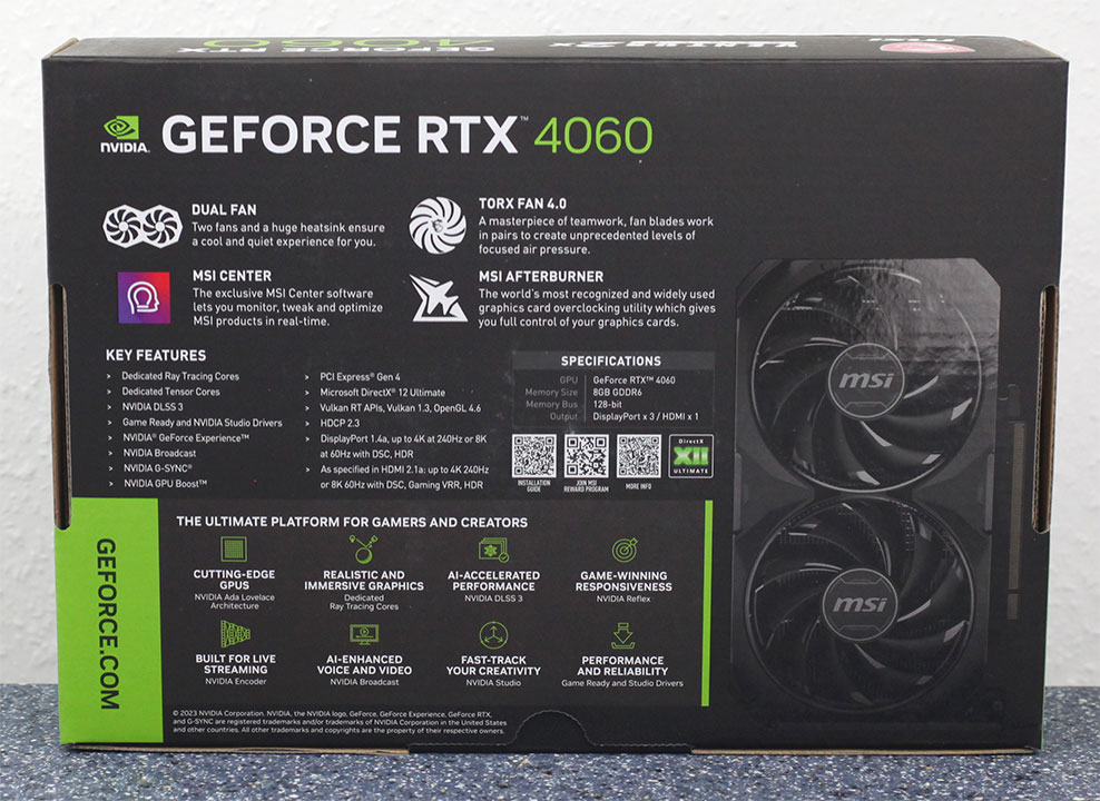
The MSI GeForce RTX 4060 Ventus 2X is being offered at the NVIDIA MSRP (baseline pricing) of $299, it's designed for those that want the most affordable RTX 4060 that they can just install and forget about, so you get the full RTX 4060 experience, without the bells-and-whistles of RGB lighting, elaborate cooling, etc. The card even comes with a small factory overclock to 2595 MHz rated boost, a 135 MHz increase. Its compact form should make it highly compatible with compact cases, including SFF ones. The 1-pound cooling solution looks plenty for the 115 W typical power, and uses a dual-fan setup. Today (June 28), NVIDIA is allowing us to publish reviews of all the RTX 4060 graphics cards priced at the $299 MSRP, we'll have reviews of more premium cards priced above the MSRP tomorrow.
Short 10-Minute Video Comparing 10x RTX 4060
Our goal with the videos is to create short summaries, not go into all the details and test results, which can be found in our written reviews.
| Price | Cores | ROPs | Core Clock | Boost Clock | Memory Clock | GPU | Transistors | Memory | |
|---|---|---|---|---|---|---|---|---|---|
| RX 6500 XT | $150 | 1024 | 32 | 2685 MHz | 2825 MHz | 2248 MHz | Navi 24 | 5400M | 4 GB, GDDR6, 64-bit |
| RTX 2060 | $170 | 1920 | 48 | 1365 MHz | 1680 MHz | 1750 MHz | TU106 | 10800M | 6 GB, GDDR6, 192-bit |
| RX 5700 XT | $150 | 2560 | 64 | 1605 MHz | 1755 MHz | 1750 MHz | Navi 10 | 10300M | 8 GB, GDDR6, 256-bit |
| RTX 3050 | $210 | 2560 | 32 | 1552 MHz | 1777 MHz | 1750 MHz | GA106 | 12000M | 8 GB, GDDR6, 128-bit |
| RTX 2070 | $210 | 2304 | 64 | 1410 MHz | 1620 MHz | 1750 MHz | TU106 | 10800M | 8 GB, GDDR6, 256-bit |
| Arc A750 | $240 | 3584 | 112 | 2050 MHz | N/A | 2000 MHz | ACM-G10 | 21700M | 8 GB, GDDR6, 256-bit |
| RX 6600 | $170 | 1792 | 64 | 2044 MHz | 2491 MHz | 1750 MHz | Navi 23 | 11060M | 8 GB, GDDR6, 128-bit |
| RX 6600 XT | $210 | 2048 | 64 | 2359 MHz | 2589 MHz | 2000 MHz | Navi 23 | 11060M | 8 GB, GDDR6, 128-bit |
| RTX 3060 | $260 | 3584 | 48 | 1320 MHz | 1777 MHz | 1875 MHz | GA106 | 12000M | 12 GB, GDDR6, 192-bit |
| RX 7600 | $250 | 2048 | 64 | 2250 MHz | 2625 MHz | 2250 MHz | Navi 33 | 13300M | 8 GB, GDDR6, 128-bit |
| RTX 4060 | $300 | 3072 | 48 | 1830 MHz | 2460 MHz | 2125 MHz | AD107 | 18900M | 8 GB, GDDR6, 128-bit |
| MSI RTX 4060 Ventus 2X | $300 | 3072 | 48 | 1830 MHz | 2595 MHz | 2125 MHz | AD107 | 18900M | 8 GB, GDDR6, 128-bit |
| Arc A770 | $290 | 4096 | 128 | 2100 MHz | N/A | 2187 MHz | ACM-G10 | 21700M | 16 GB, GDDR6, 256-bit |
| RTX 2080 | $240 | 2944 | 64 | 1515 MHz | 1710 MHz | 1750 MHz | TU104 | 13600M | 8 GB, GDDR6, 256-bit |
| RTX 3060 Ti | $300 | 4864 | 80 | 1410 MHz | 1665 MHz | 1750 MHz | GA104 | 17400M | 8 GB, GDDR6, 256-bit |
| RTX 4060 Ti | $380 | 4352 | 48 | 2310 MHz | 2535 MHz | 2250 MHz | AD106 | 22900M | 8 GB, GDDR6, 128-bit |
| RX 6700 XT | $310 | 2560 | 64 | 2424 MHz | 2581 MHz | 2000 MHz | Navi 22 | 17200M | 12 GB, GDDR6, 192-bit |
| RTX 2080 Ti | $380 | 4352 | 88 | 1350 MHz | 1545 MHz | 1750 MHz | TU102 | 18600M | 11 GB, GDDR6, 352-bit |
| RTX 3070 | $320 | 5888 | 96 | 1500 MHz | 1725 MHz | 1750 MHz | GA104 | 17400M | 8 GB, GDDR6, 256-bit |
| RTX 3070 Ti | $400 | 6144 | 96 | 1575 MHz | 1770 MHz | 1188 MHz | GA104 | 17400M | 8 GB, GDDR6X, 256-bit |
| RX 6800 | $430 | 3840 | 96 | 1815 MHz | 2105 MHz | 2000 MHz | Navi 21 | 26800M | 16 GB, GDDR6, 256-bit |
Architecture
The Ada graphics architecture heralds the third generation of the NVIDIA RTX technology, an effort toward increasing the realism of game visuals by leveraging real-time ray tracing, without the enormous amount of compute power required to draw purely ray-traced 3D graphics. This is done by blending conventional raster graphics with ray traced elements such as reflections, lighting, and global illumination, to name a few. The 3rd generation of RTX introduces the new higher IPC "Ada" CUDA core, 3rd generation RT core, 4th generation Tensor core, and the new Optical Flow Processor, a component that plays a key role in generating new frames without involving the GPU's main graphics rendering pipeline.


The GeForce Ada graphics architecture driving the RTX 4060 leverages the TSMC 5 nm EUV foundry process to increase transistor counts. At the heart of this GPU is the new AD107 silicon, with a transistor count of 18.9 billion, which is almost 60% higher than that of the previous-generation GA106, and about 9% more than the GA104. The GPU features a generationally narrower PCI-Express 4.0 x8 host interface, and a 128-bit wide GDDR6 memory interface. This is causing some controversy, and we'll present NVIDIA's explanation below. The Optical Flow Accelerator (OFA) is an independent top-level component. For the RTX 4060, the chip features one 8th Gen NVENC and one 5th Gen NVDEC unit, including hardware-acceleration for the AV1 format.
The essential component hierarchy is similar to past generations of NVIDIA GPUs. The AD107 silicon features 3 Graphics Processing Clusters (GPCs), each of these has all the SIMD and graphics rendering machinery, and is a small GPU in its own right. Each GPC shares a raster engine (geometry processing components) and two ROP partitions (each with eight ROP units). The GPC of the AD107 contains four Texture Processing Clusters (TPCs), the main number-crunching machinery. Each of these has two Streaming Multiprocessors (SM), and a Polymorph unit. Each SM contains 128 CUDA cores across four partitions. Half of these CUDA cores are pure-FP32; while the other half is capable of FP32 or INT32. The SM retains concurrent FP32+INT32 math processing capability. The SM also contains a 3rd generation RT core, four 4th generation Tensor cores, some cache memory, and four TMUs. There are 8 SM per GPC, so 1,024 CUDA cores, 32 Tensor cores, and 8 RT cores; per GPC. There are three such GPCs, which add up to 3,072 CUDA cores, 96 TMUs, 96 Tensor Cores, and 24 RT cores. There are 48 ROPs on the silicon. The AD107 features a 24 MB L2 cache, which is smaller than the 32 MB on the AD106 powering the RTX 4060 Ti.
3rd Gen RT Core and Ray Tracing


The 3rd generation RT core accelerates the most math-intensive aspects of real-time ray tracing, including BVH traversal. Displaced micro-mesh engine is a revolutionary feature introduced with the new 3rd generation RT core. Just as mesh shaders and tessellation have had a profound impact on improving performance with complex raster geometry, allowing game developers to significantly increase geometric complexity; DMMs is a method to reduce the complexity of the bounding-volume hierarchy (BVH) data-structure, which is used to determine where a ray hits geometry. Previously, the BVH had to capture even the smallest details to properly determine the intersection point. Ada's ray tracing architecture also receives a major performance uplift from Shader Execution Reordering (SER), a software-defined feature that requires awareness from game-engines, to help the GPU reorganize and optimize worker threads associated with ray tracing.


The BVH now needn't have data for every single triangle on an object, but can represent objects with complex geometry as a coarse mesh of base triangles, which greatly simplifies the BVH data structure. A simpler BVH means less memory consumed and helps to greatly reduce ray tracing CPU load, because the CPU only has to generate a smaller structure. With older "Ampere" and "Turing" RT cores, each triangle on an object had to be sampled at high overhead, so the RT core could precisely calculate ray intersection for each triangle. With Ada, the simpler BVH, plus the displacement maps can be sent to the RT core, which is now able to figure out the exact hit point on its own. NVIDIA has seen 11:1 to 28:1 compression in total triangle counts. This reduces BVH compile times by 7.6x to over 15x, in comparison to the older RT core; and reducing its storage footprint by anywhere between 6.5 to 20 times. DMMs could reduce disk- and memory bandwidth utilization, utilization of the PCIe bus, as well as reduce CPU utilization. NVIDIA worked with Simplygon and Adobe to add DMM support for their tool chains.
Opacity Micro Meshes


Opacity Micro Meshes (OMM) is a new feature introduced with Ada to improve rasterization performance, particularly with objects that have alpha (transparency data). Most low-priority objects in a 3D scene, such as leaves on a tree, are essentially rectangles with textures on the leaves where the transparency (alpha) creates the shape of the leaf. RT cores have a hard time intersecting rays with such objects, because they're not really in the shape that they appear (they're really just rectangles with textures that give you the illusion of shape). Previous-generation RT cores had to have multiple interactions with the rendering stage to figure out the shape of a transparent object, because they couldn't test for alpha by themselves.


This has been solved by using OMMs. Just as DMMs simplify geometry by creating meshes of micro-triangles; OMMs create meshes of rectangular textures that align with parts of the texture that aren't alpha, so the RT core has a better understanding of the geometry of the object, and can correctly calculate ray intersections. This has a significant performance impact on shading performance in non-RT applications, too. Practical applications of OMMs aren't just low-priority objects such as vegetation, but also smoke-sprites and localized fog. Traditionally there was a lot of overdraw for such effects, because they layered multiple textures on top of each other, that all had to be fully processed by the shaders. Now only the non-opaque pixels get executed—OMMs provide a 30 percent speedup with graphics buffer fill-rates, and a 10 percent impact on frame-rates.
DLSS 3 Frame Generation
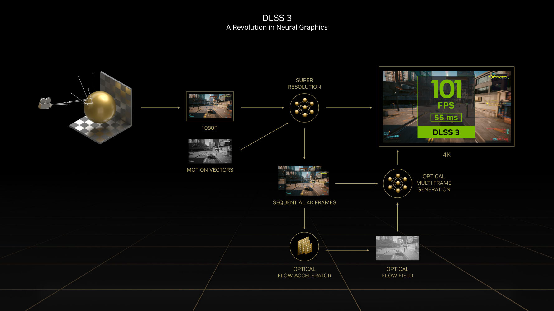

DLSS 3 introduces a revolutionary new feature that promises a doubling in frame-rate at comparable quality, it's called AI frame-generation. Building on DLSS 2 and its AI super-resolution (scaling up a lower-resolution frame to native resolution with minimal quality loss); DLSS 3 can generate entire frames simply using AI, without involving the graphics rendering pipeline, it's also possible to enable frame generation at native resolution without upscaling. Later in the article, we will show you DLSS 3 in action.


Every alternating frame with DLSS 3 is hence AI-generated, without being a replica of the previous rendered frame. This is possible only on the Ada graphics architecture, because of a hardware component called the optical flow accelerator (OFA), which assists in predicting what the next frame could look like, by creating what NVIDIA calls an optical flow-field. OFA ensures that the DLSS 3 algorithm isn't confused by static objects in a rapidly-changing 3D scene (such as a race sim). The process heavily relies on the performance uplift introduced by the FP8 math format of the 4th generation Tensor core. A third key ingredient of DLSS 3 is Reflex. By reducing the rendering queue to zero, Reflex plays a vital role in ensuring that latency with DLSS 3 enabled is at an acceptable level. A combination of OFA and the 4th Gen Tensor core is why the Ada architecture is required to use DLSS 3, and why it won't work on older architectures.
Ada Rebalanced Memory Subsystem


The previous-generation GeForce RTX 3060 featured a 192-bit wide GDDR6 memory interface driving its 12 GB of 14 Gbps-rated GDDR6 memory, which has caused some controversy with the RTX 4060 using a narrower 128-bit wide memory interface to drive 8 GB of 17 Gbps memory. With the new Ada Lovelace graphics architecture, NVIDIA has tried to re-balance the memory sub-system such that there's dependence on larger on-die caches, allowing NVIDIA to narrow down the GPU's GDDR6 memory interface. The obvious benefit of this to NVIDIA is reduced costs, let's make no mistake about it, but NVIDIA maintains that this isn't a big problem for the GPU.
The last-level cache, or L2 cache, of NVIDIA Ada GPUs is anywhere between 8-10 times larger than the ones on the previous-generation Ampere GPUs. The AD107 silicon powering the RTX 4060 has a 24 MB L2 cache, compared to the 2 MB of the GA107 silicon powering the RTX 3050, and 3 MB of the GA106 powering the RTX 3060. NVIDIA illustrated an example of how the larger on-die LLC reduces video memory pressure (trips to GDDR6) by anywhere between 40% to 60% on the same GPU, by soaking up a larger number of memory access requests by the shaders.
The L2 cache is unified victim cache to the GPU's various GPCs and their local TPCs. Data that isn't hot enough (frequently accessed enough) to be resident on the small L1 caches of the SM, is ejected to the L2 cache, and depending on its heat, pushed to the GDDR6 video memory. The L2 cache is an order of magnitude faster than than video memory in terms of latency, and so having frequently-accessed data reside there offers a considerable benefit.

As we mentioned earlier from NVIDIA's claims, this re-balancing of the memory sub-system between the on-die LLC and video memory lowers the GPU's access to the latter by as much as 60%, which means the GPU can make do with a narrower 128-bit wide GDDR6 memory bus. NVIDIA has used generationally faster 17 Gbps memory chips in the RTX 4060. NVIDIA developed a new means of presenting the memory bandwidth that takes into account the contribution of the L2 cache, its hit-rate, and the consequent reduction in video memory traffic. While the memory bandwidth of the RTX 4060 is 272 GB/s, NVIDIA claims that its "effective bandwidth" is 453 GB/s. It's interesting to point out that NVIDIA has used "effective bandwidth" figures in the past to highlight its lossless memory compression technologies, but has never been this vocal about it.
Packaging
Our Patreon Silver Supporters can read articles in single-page format.
Aug 1st, 2025 15:48 CDT
change timezone
Latest GPU Drivers
New Forum Posts
- Samsung 870 EVO - Beware, certain batches prone to failure! (1302)
- AMD Radeon 6900 XT Limited Black Edition Bios Problems - Boost Problems (9)
- Have you got pie today? (16818)
- WCG Daily Numbers (12955)
- What are you playing? (24029)
- Blender 4.0.1 BMW27 demo test (22)
- Can't find vbios for Rx 470 (6)
- TPU's Rosetta Milestones and Daily Pie Thread (2419)
- Folding Pie and Milestones!! (9661)
- 3DMARK "LEGENDARY" (357)
Popular Reviews
- MSI Claw 8 AI+ A2VM Review
- Lenovo Legion 5i (15IRX10) Review - Feature-Rich and Wallet Friendly
- ASUS ROG Crosshair X870E Apex Review
- Herman Miller Logitech G Embody Review - No Pain, No Gain
- Orbital Pathfinder Review
- Montech X5 Review
- Upcoming Hardware Launches 2025 (Updated May 2025)
- Lian Li O11 Dynamic Mini V2 Review
- Noctua NF-A12x25 G2 PWM Fan Review
- AMD Ryzen 7 9800X3D Review - The Best Gaming Processor
TPU on YouTube
Controversial News Posts
- AMD's Upcoming UDNA / RDNA 5 GPU Could Feature 96 CUs and 384-bit Memory Bus (137)
- AMD Radeon RX 9070 XT Gains 9% Performance at 1440p with Latest Driver, Beats RTX 5070 Ti (131)
- Intel "Nova Lake-S" Core Ultra 3, Ultra 5, Ultra 7, and Ultra 9 Core Configurations Surface (110)
- DDR6 Memory Arrives in 2027 with 8,800-17,600 MT/s Speeds (102)
- NVIDIA to Debut GeForce RTX 50-series SUPER GPUs by Christmas (101)
- AMD Sampling Next-Gen Ryzen Desktop "Medusa Ridge," Sees Incremental IPC Upgrade, New cIOD (97)
- Intel CEO Confirms SMT To Return to Future CPUs (95)
- NVIDIA Becomes First Company Ever to Hit $4 Trillion Market-Cap (94)