 34
34
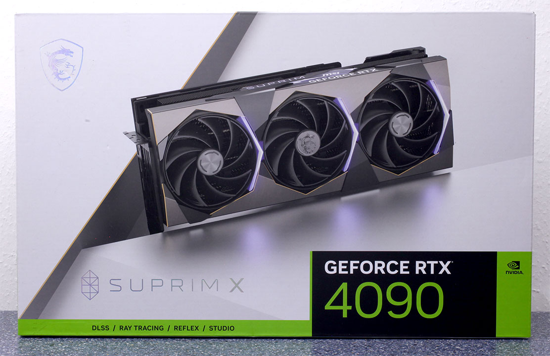
MSI GeForce RTX 4090 Suprim X Review
(34 Comments) »Introduction
MSI GeForce RTX 4090 Suprim X is the company's flagship air-cooled graphics card, based on NVIDIA's new flagship GPU, the RTX 4090 "Ada Lovelace," which we've extensively reviewed for you today across as many brands as we could get our hands on. The Suprim Liquid X builds on the short legacy of MSI's refreshing new Suprim graphics card brand, which replaced the Lightning and Gaming Z brands at the top of MSI's product stack. Slick, subtle styling, and rich materials are the new standard. Suprim is MSI's attempt at outdoing NVIDIA's Founders Edition in product design, without losing sight of MSI's main objective—to be the fastest graphics card out of the box, with the highest headroom and features for enthusiasts. This review will tell you just how far MSI goes to meet this goal. We're also reviewing the liquid-cooled sibling of this card, the RTX 4090 Suprim Liquid X.

The GeForce RTX 4090 is currently the most powerful GPU on the market, and the flagship of the RTX 40-series "Ada." Leveraging the 5 nm EUV process, the new "Ada" graphics architecture more than triples the transistor-counts, to create newer fixed-function accelerators, more on-die cache, and a near-doubling in the SIMD machinery of the GPU over what the RTX 3090 comes with. The idea here is to offer a roughly 50% performance uplift over the RTX 3090, and a nearly 2x uplift over the RTX 3080 (which NVIDIA considered its previous-gen flagship).
The RTX 4090 is based on the 5 nm Ada AD102 silicon, with an incredible 76 billion transistor-count, triple that of its predecessor while actually being physically smaller; and fitting into the same power envelope, with 450 W typical board power. NVIDIA carved the RTX 4090 out of the AD102 silicon by enabling 128 out of 144 SM, or 16,384 out of 18,432 CUDA cores; 128 RT cores, 512 Tensor cores, 512 TMUs, and 192 ROPs. The memory configuration is unchanged, with 24 GB of 21 Gbps GDDR6X memory across a 384-bit wide bus. Besides making real time ray tracing have a much lower performance impact than enabling it did with the previous-generation; NVIDIA also introduced AI total frame-generation using DLSS 3, wherein unique frames are generated by AI, without involving the graphics rendering hardware.
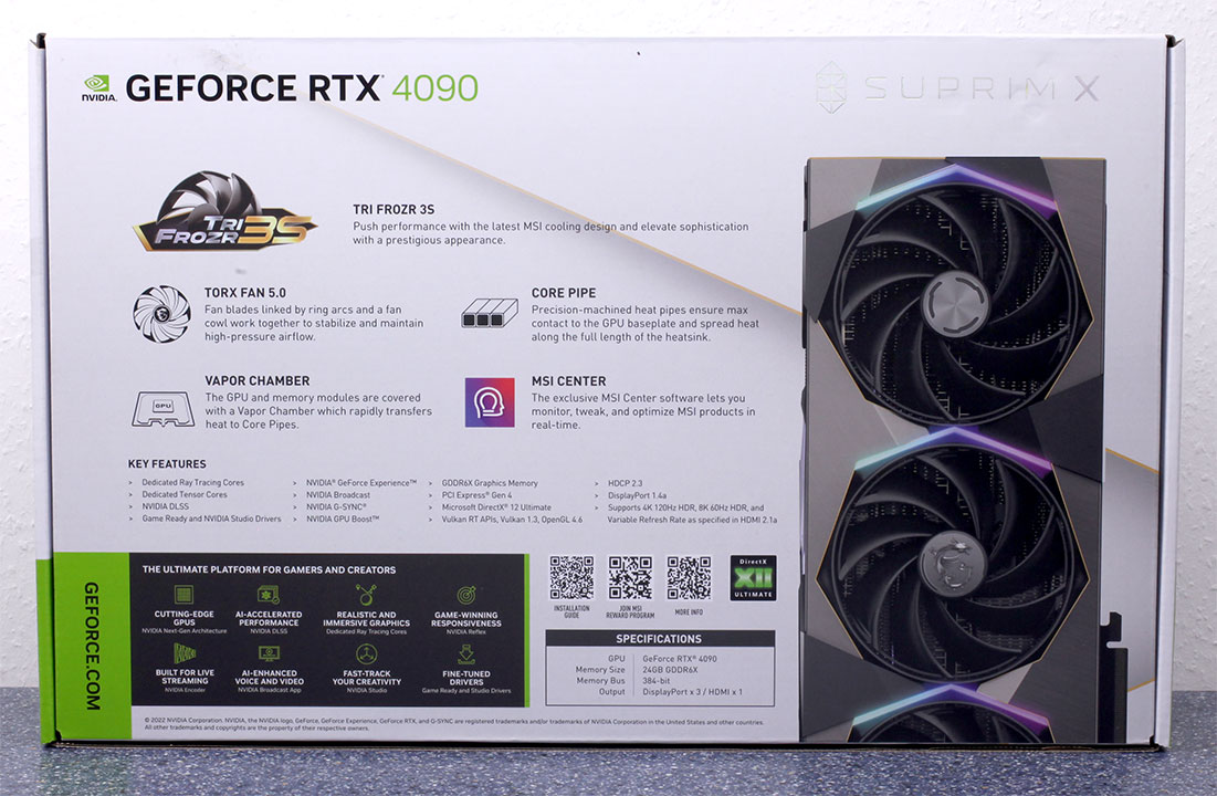
The MSI RTX 4090 Suprim X uses a stunning-looking 4-slot cooling solution that's made of premium multi-tone alloys, with a powerful aluminium fin-stack heatsink underneath. This is a conventional air-cooled solution unlike the Suprim Liquid X; and uses a trio of fans. MSI has given the card a healthy overclock of 2.62 GHz compared to 2.52 GHz reference, which interestingly is the same factory-OC as the liquid-cooled card. MSI is pricing this card at $1,700, a mere $100 premium over the $1600 NVIDIA baseline.
| Price | Cores | ROPs | Core Clock | Boost Clock | Memory Clock | GPU | Transistors | Memory | |
|---|---|---|---|---|---|---|---|---|---|
| RTX 2080 | $400 | 2944 | 64 | 1515 MHz | 1710 MHz | 1750 MHz | TU104 | 13600M | 8 GB, GDDR6, 256-bit |
| RTX 3060 Ti | $450 | 4864 | 80 | 1410 MHz | 1665 MHz | 1750 MHz | GA104 | 17400M | 8 GB, GDDR6, 256-bit |
| RX 6700 XT | $410 | 2560 | 64 | 2424 MHz | 2581 MHz | 2000 MHz | Navi 22 | 17200M | 12 GB, GDDR6, 192-bit |
| RX 6750 XT | $470 | 2560 | 64 | 2495 MHz | 2600 MHz | 2250 MHz | Navi 22 | 17200M | 12 GB, GDDR6, 192-bit |
| RTX 2080 Ti | $550 | 4352 | 88 | 1350 MHz | 1545 MHz | 1750 MHz | TU102 | 18600M | 11 GB, GDDR6, 352-bit |
| RTX 3070 | $530 | 5888 | 96 | 1500 MHz | 1725 MHz | 1750 MHz | GA104 | 17400M | 8 GB, GDDR6, 256-bit |
| RTX 3070 Ti | $600 | 6144 | 96 | 1575 MHz | 1770 MHz | 1188 MHz | GA104 | 17400M | 8 GB, GDDR6X, 256-bit |
| RX 6800 | $580 | 3840 | 96 | 1815 MHz | 2105 MHz | 2000 MHz | Navi 21 | 26800M | 16 GB, GDDR6, 256-bit |
| RX 6800 XT | $600 | 4608 | 128 | 2015 MHz | 2250 MHz | 2000 MHz | Navi 21 | 26800M | 16 GB, GDDR6, 256-bit |
| RTX 3080 | $660 | 8704 | 96 | 1440 MHz | 1710 MHz | 1188 MHz | GA102 | 28000M | 10 GB, GDDR6X, 320-bit |
| RTX 3080 Ti | $850 | 10240 | 112 | 1365 MHz | 1665 MHz | 1188 MHz | GA102 | 28000M | 12 GB, GDDR6X, 384-bit |
| RX 6900 XT | $680 | 5120 | 128 | 2015 MHz | 2250 MHz | 2000 MHz | Navi 21 | 26800M | 16 GB, GDDR6, 256-bit |
| RX 6950 XT | $950 | 5120 | 128 | 2100 MHz | 2310 MHz | 2250 MHz | Navi 21 | 26800M | 16 GB, GDDR6, 256-bit |
| RTX 3090 | $950 | 10496 | 112 | 1395 MHz | 1695 MHz | 1219 MHz | GA102 | 28000M | 24 GB, GDDR6X, 384-bit |
| RTX 3090 Ti | $1200 | 10752 | 112 | 1560 MHz | 1950 MHz | 1313 MHz | GA102 | 28000M | 24 GB, GDDR6X, 384-bit |
| RTX 4090 | $1600 | 16384 | 176 | 2235 MHz | 2520 MHz | 1313 MHz | AD102 | 76300M | 24 GB, GDDR6X, 384-bit |
| MSI RTX 4090 Suprim X | $1700 | 16384 | 176 | 2235 MHz | 2625 MHz | 1313 MHz | AD102 | 76300M | 24 GB, GDDR6X, 384-bit |
GeForce Ada Architecture
The Ada graphics architecture heralds the third generation of the NVIDIA RTX technology, an effort toward increasing the realism in game visuals by leveraging real-time ray tracing, without the enormous amount of compute power required to draw purely ray-traced 3D graphics. This is done by blending conventional raster graphics with ray traced elements such as reflections, lighting, and global illumination, to name a few. The 3rd generation of RTX heralds the new higher IPC "Ada" CUDA core, 3rd generation RT core, 4th generation Tensor core, and the new Optical Flow Processor, a component that plays a key role in generating new frames without involving the GPU's main graphics rendering pipeline.

The GeForce Ada graphics architecture driving the RTX 4090 leverages the TSMC 5 nm EUV foundry process to increase transistor counts to a mammoth 76.3 billion transistors, a nearly 3-fold increase over the previous-generation; while the die-size is actually smaller, at 608 mm² compared to 628 mm² of the previous-generation GA102. The GPU features a PCI-Express 4.0 x16 host interface, and a 384-bit wide GDDR6X memory bus, which on the RTX 4090 wires out to 24 GB of memory. The Optical Flow Accelerator (OFA) is an independent top-level component. The chip features two NVENC and one NVDEC units in the GeForce RTX 40-series; while future professional-visualization graphics cards will have all six each of the NVENC and NVDEC components enabled.
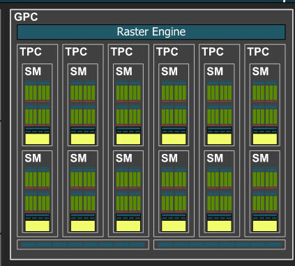
The essential component hierarchy is similar to past generations of NVIDIA GPUs. The AD102 silicon features a whopping 12 Graphics Processing Clusters (GPCs), each of these has all the SIMD and graphics rendering machinery, and is a small GPU in its own right. Each GPC shares a raster engine (geometry processing components) and two ROP partitions (each with eight ROP units). The GPC of the AD102 contains six Texture Processing Clusters (TPCs), the main number-crunching machinery. Each of these has two Streaming Multiprocessors (SM), and a Polymorph unit. Each SM contains 128 CUDA cores across four partitions. Half of these CUDA cores are pure-FP32; while the other half is capable of FP32 or INT32. The SM retains concurrent FP32+INT32 math processing capability. The SM also contains a 3rd generation RT core, four 4th generation Tensor cores, some cache memory, and four TMUs. There are 12 SM per GPC, so 1,536 CUDA cores, 48 Tensor cores, and 12 RT cores; per GPC. Twelve GPCs hence add up to 18,432 CUDA cores, 576 Tensor cores, and 144 RT cores. Each GPC contributes 16 ROPs, so there are a mammoth 192 ROPs on the silicon. A 96 MB L2 cache serves as town-square for the various GPCs, memory controllers, and the PCIe host interface, to exchange data. NVIDIA carved the RTX 4090 out of the AD102 by disabling one of the twelve GPCs, and a further two TPCs from two of the other GPCs, as shown in the red-shaded parts of the block diagram above. The RTX 4090 has 72 MB L2 cache enabled (out of 96 MB physically present on the silicon).


The 3rd generation RT core accelerates the most math-intensive aspects of real-time ray tracing, including BVH traversal. Displaced micro-mesh engine is a revolutionary feature introduced with the new 3rd generation RT core, which accelerates the displaced micro-mesh feature. Just as mesh shaders and tessellation have had a profound impact on improving performance with complex raster geometry, allowing game developers to significantly increase geometric complexity; DMMs is a method to reduce the complexity of the bounding-volume hierarchy (BVH) data-structure, which is used to determine where a ray hits geometry. Previously the BVH had to capture even the smallest details to properly determine the intersection point. Ada's ray tracing architecture receives a major performance uplift from Shader Execution Reordering (SER), a software-defined feature that requires awareness from game-engines, to help the GPU reorganize and optimize worker threads associated with ray tracing.


The BVH now needn't have data for every single triangle on an object, but can represent objects with complex geometry as a coarse mesh of base triangles, which greatly simplifies the BVH data structure. A simpler BVH means less memory consumed and helps to greatly reduce ray tracing CPU load, because the CPU only has to generate a smaller structure. With older "Ampere" and "Turing" RT cores, each triangle on an object had to be sampled at high overhead, so the RT core could precisely calculate ray intersection for each triangle. With Ada, the simpler BVH, plus the displacement maps can be sent to the RT core, which is now able to figure out the exact hit point on its own. NVIDIA has seen 11:1 to 28:1 compression in total triangle counts. This reduces BVH compile times by 7.6x to over 15x, in comparison to the older RT core; and reducing its storage footprint by anywhere between 6.5 to 20 times. DMMs could reduce disk- and memory bandwidth utilization, utilization of the PCIe bus, as well as reduce CPU utilization. NVIDIA worked with Simplygon and Adobe to add DMM support for their tool chains.

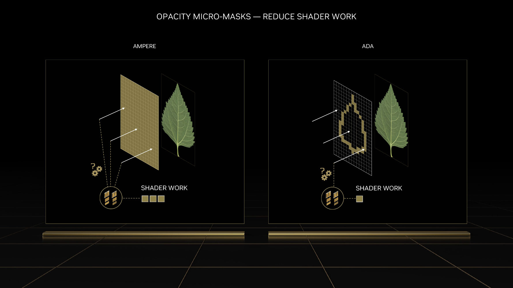
Opacity Micro Meshes (OMM) is a new feature introduced with Ada to improve rasterization performance, particularly with objects that have alpha (transparency data). Most low-priority objects in a 3D scene, such as leaves on a tree, are essentially rectangles with textures on the leaves where the transparency (alpha) creates the shape of the leaf. RT cores have a hard time intersecting rays with such objects, because they're not really in the shape that they appear (they're really just rectangles with textures that give you the illusion of shape). Previous-generation RT cores had to have multiple interactions with the rendering stage to figure out the shape of a transparent object, because they couldn't test for alpha by themselves.
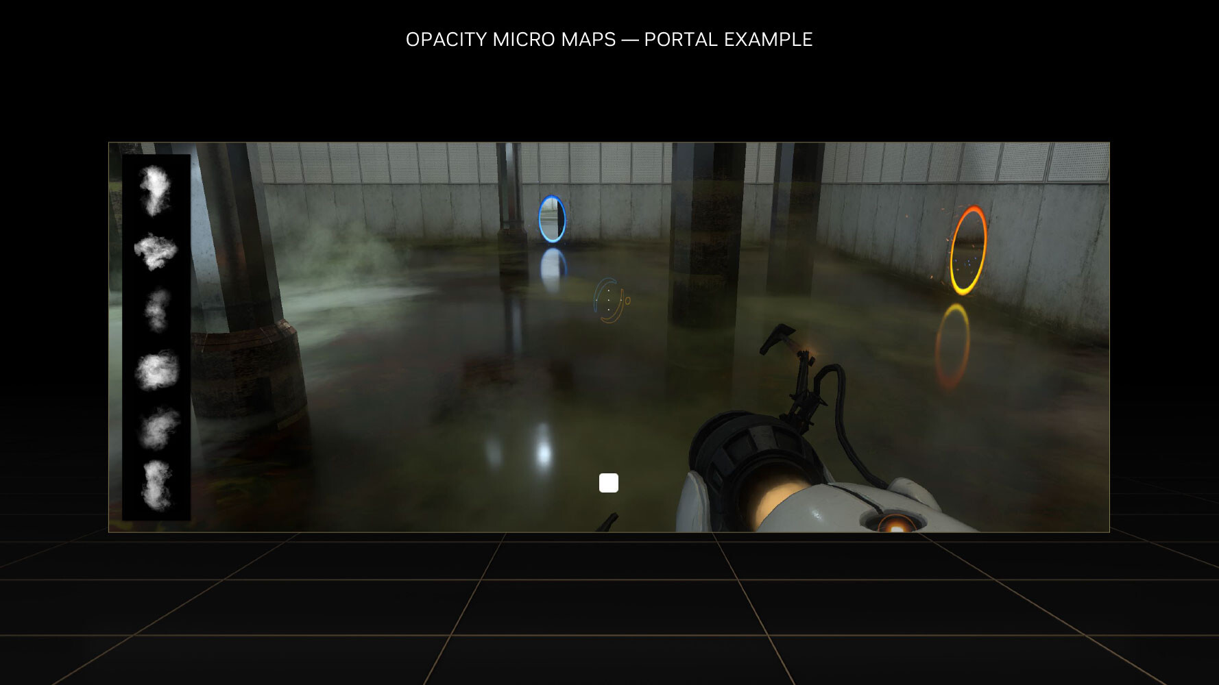
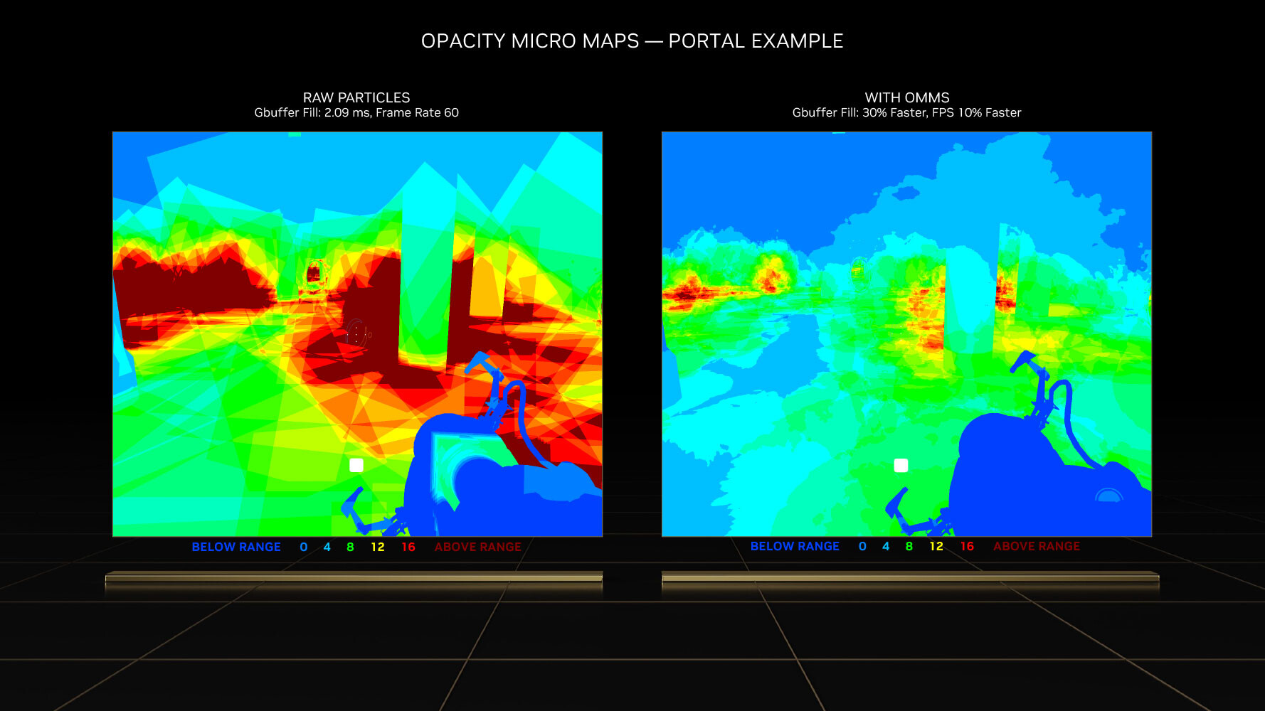
This has been solved by using OMMs. Just as DMMs simplify geometry by creating meshes of micro-triangles; OMMs create meshes of rectangular textures that align with parts of the texture that aren't alpha, so the RT core has a better understanding of the geometry of the object, and can correctly calculate ray intersections. This has a significant performance impact on shading performance in non-RT applications, too. Practical applications of OMMs aren't just low-priority objects such as vegetation, but also smoke-sprites and localized fog. Traditionally there was a lot of overdraw for such effects, because they layered multiple textures on top of each other, that all had to be fully processed by the shaders. Now only the non-opaque pixels get executed—OMMs provide a 30 percent speedup with graphics buffer fill-rates, and a 10 percent impact on frame-rates.


DLSS 3 introduces a revolutionary new feature that promises a doubling in frame-rate at comparable quality, it's called AI frame-generation. While it has all the features of DLSS 2 and its AI super-resolution (scaling up a lower-resolution frame to native resolution with minimal quality loss); DLSS 3 can generate entire frames simply using AI, without involving the graphics rendering pipeline.
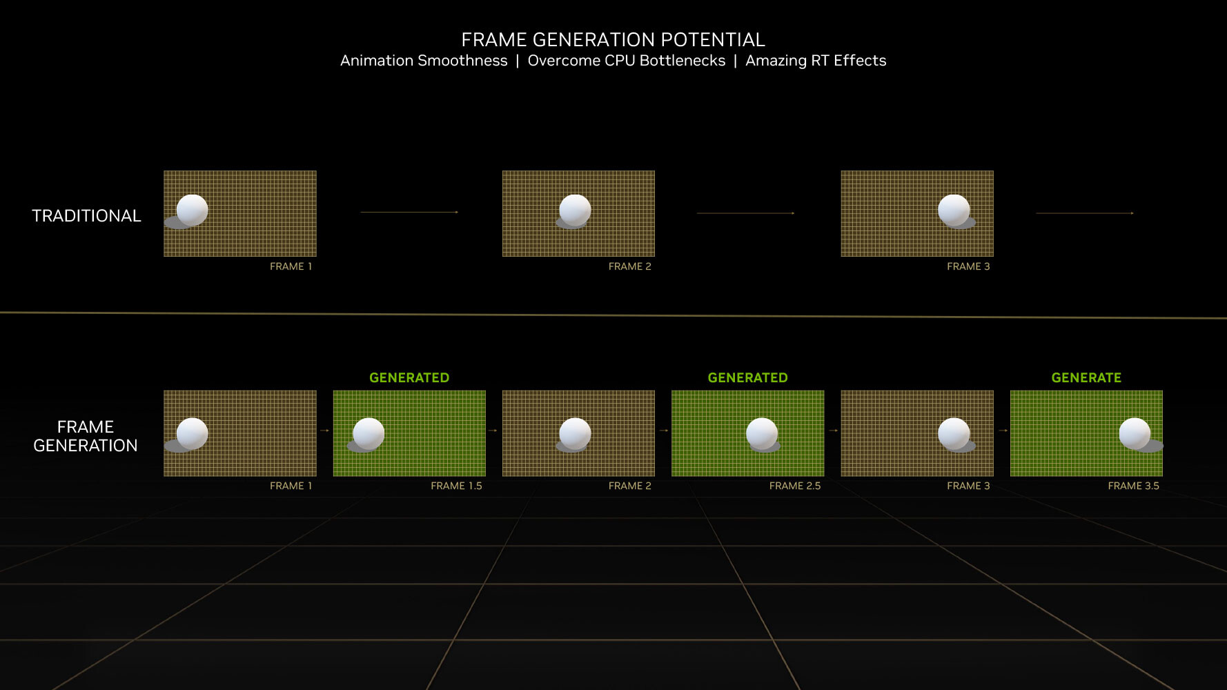
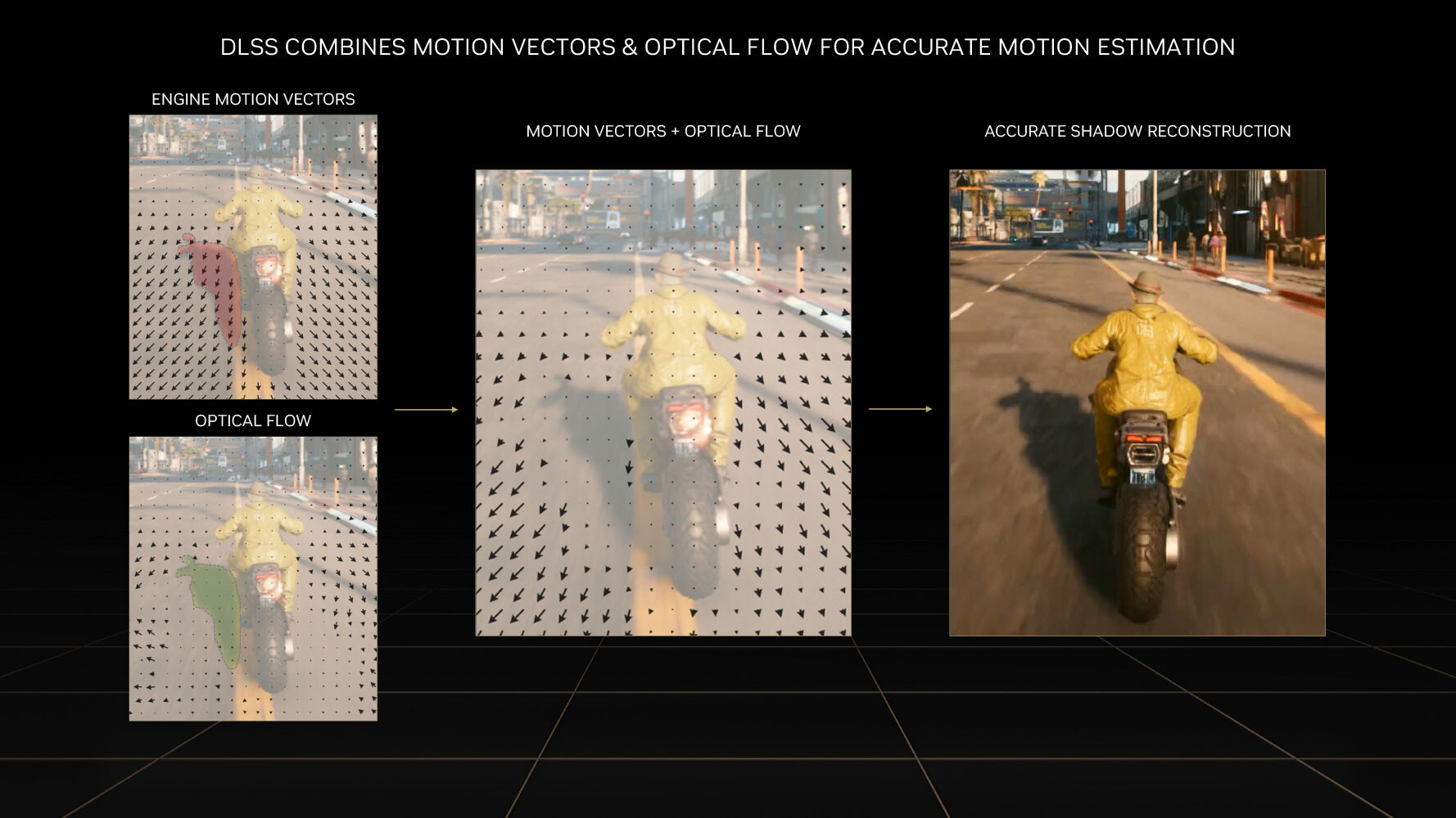
Every alternating frame with DLSS 3 is hence AI-generated, without being a replica of the previous rendered frame. This is possible only on the Ada graphics architecture, because of a hardware component called the optical flow accelerator (OFA), which assists in predicting what the next frame could look like, by creating what NVIDIA calls an optical flow-field. OFA ensures that the DLSS 3 algorithm isn't confused by static objects in a rapidly-changing 3D scene (such as a race sim). The process heavily relies on the performance uplift introduced by the FP8 math format of the 4th generation Tensor core. A third key ingredient of DLSS 3 is Reflex. By reducing the rendering queue to zero, Reflex plays a vital role in ensuring that frame-times with DLSS 3 are at an acceptable level, and a render-queue doesn't confuse the upscaler. A combination of OFA and the 4th Gen Tensor core is why the Ada architecture is required to use DLSS 3, and why it won't work on older architectures.
Packaging
The Card


The MSI GeForce 40 Suprim Series retains most of the design elements and color theme of their GeForce 30 offerings. The dominant color is metal gray in various shades. On the back you'll find a high-quality metal backplate.
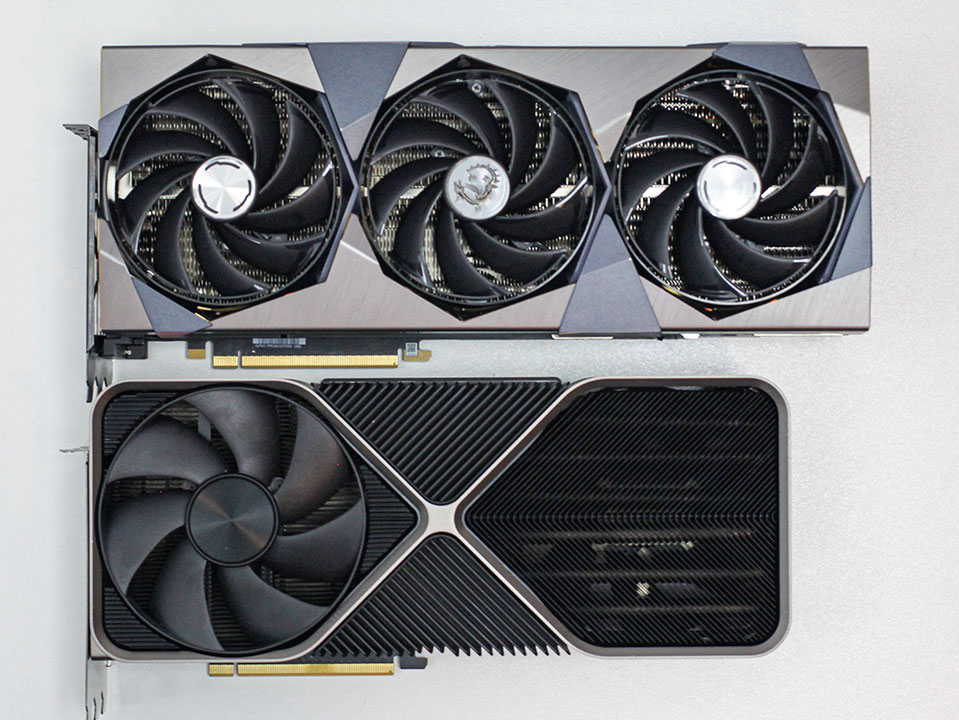

The Suprim X is considerably bigger than the NVIDIA Founders Edition.
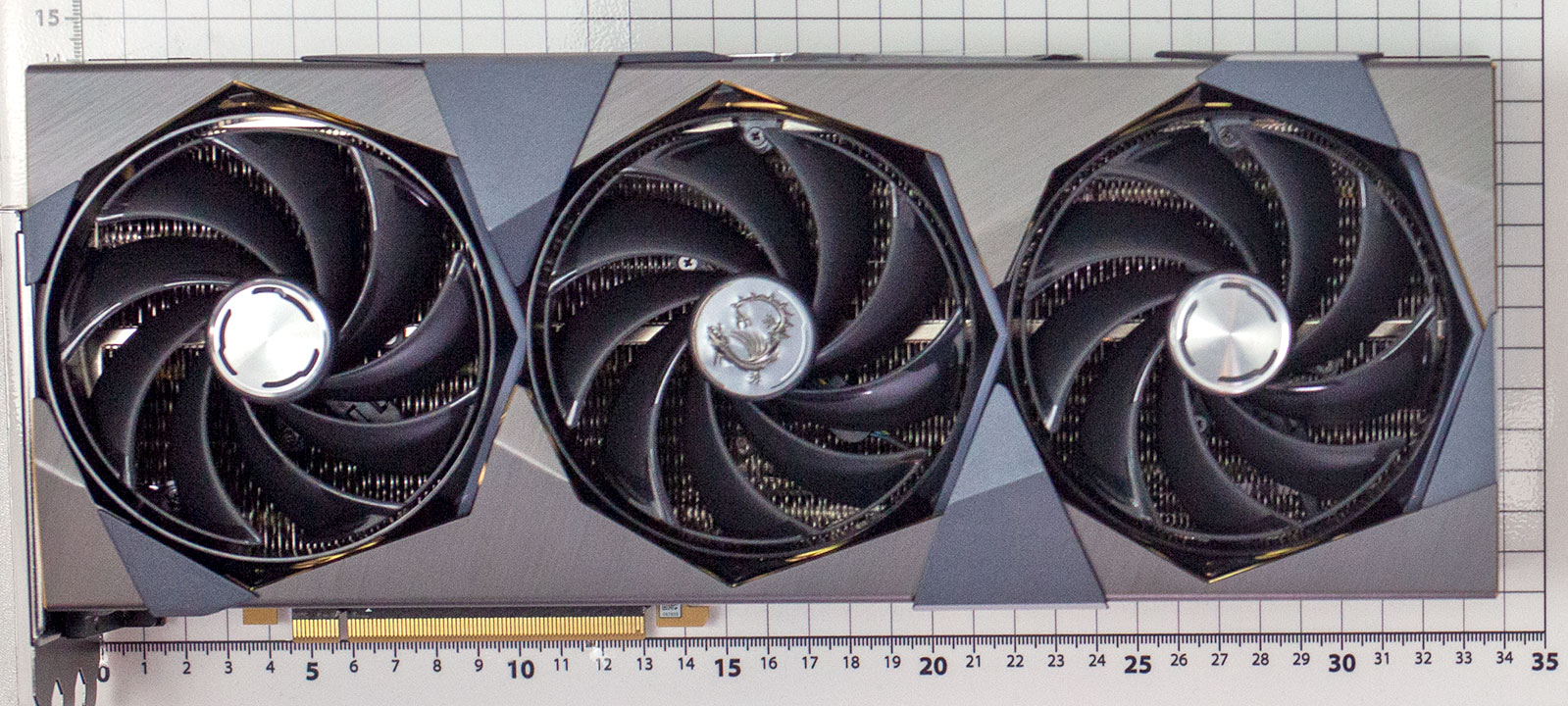
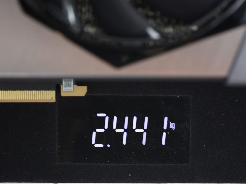
Dimensions of the card are 34.0 x 14.0 cm, and it weighs 2441 g.


Installation requires four slots in your system.

Display connectivity includes three standard DisplayPort 1.4a ports and one HDMI 2.1a (same as Ampere).
NVIDIA introduced the concept of dual NVDEC and NVENC Codecs with the Ada architecture. This means there are two independent sets of hardware-accelerators; so you can encode and decode two streams of video in parallel or one stream at double the FPS rate. The new 8th Gen NVENC now accelerates AV1 encoding, besides HEVC. You also get an "optical flow accelerator" unit that is able to calculate intermediate frames for videos, to smooth playback. The same hardware unit is used for frame generation in DLSS 3.


The card uses the new 12+4 pin ATX 12VHPWR connector, which is rated for up to 600 W of power draw. An adapter cable from 4x PCIe 8-pin is included, you can also run the card with just three 8-pins.

This dual BIOS switch lets you toggle between the default "silent" BIOS and a "gaming" BIOS with a more aggressive fan curve.
Teardown


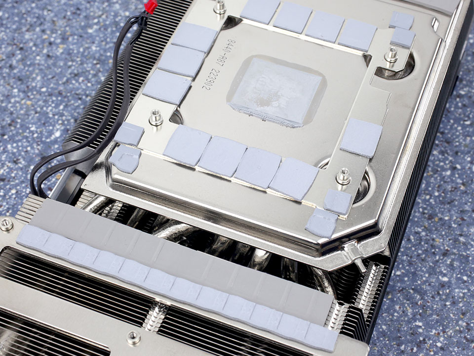
The main heatsink provides cooling for the memory GPU, memory chips and VRM circuitry. It uses a large vapor-chamber base with ten heatpipes (the 10th heatpipe goes in the other direction and wraps around).


MSI has installed a metal reinforcement brace on their card to protect against sagging.

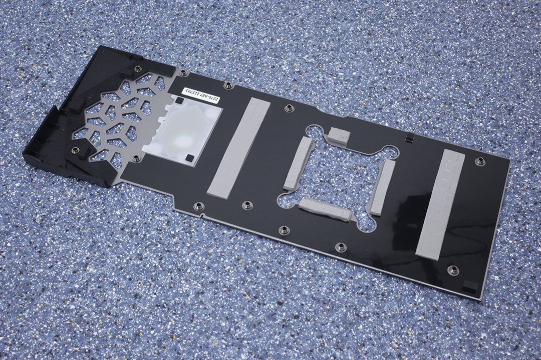
The backplate is made of metal and protects the card against damage during installation and handling.
High-resolution PCB Pictures
These pictures are for the convenience of volt modders and people who would like to see all the finer details on the PCB. Feel free to link back to us and use these in your articles, videos or forum posts.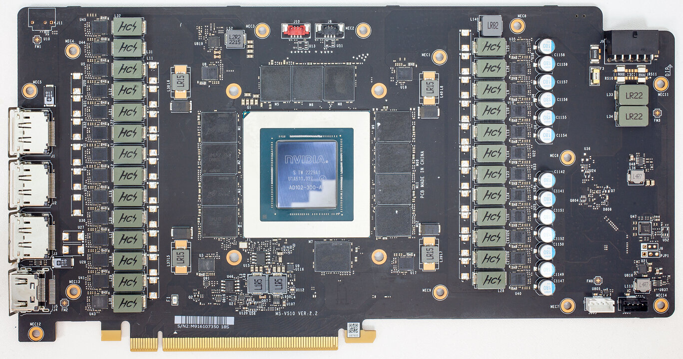

High-resolution versions are also available (front, back).
Our Patreon Silver Supporters can read articles in single-page format.
May 2nd, 2024 11:29 EDT
change timezone
Latest GPU Drivers
New Forum Posts
- Free Games Thread (3770)
- What are you playing? (20570)
- 7800x3d $216 in bundle at Microcenter (8)
- Aviation fuel, no co2 (12)
- need help with power limiting my i7-8750h (8)
- best budget freindly 5.1 soundbars in 2024 (3)
- Current Sales, Bundles, Giveaways (10225)
- What's an inexpensive AIO product line with a strong pump and low price? (97)
- Old high quality PSU, or semi-old mid-quality PSU? (43)
- TPU's Nostalgic Hardware Club (18492)
Popular Reviews
- Ugreen NASync DXP4800 Plus Review
- ASRock NUC BOX-155H (Intel Core Ultra 7 155H) Review
- Montech Sky Two GX Review
- HYTE THICC Q60 240 mm AIO Review
- Upcoming Hardware Launches 2023 (Updated Feb 2024)
- MOONDROP x Crinacle DUSK In-Ear Monitors Review - The Last 5%
- Team Group T-Force Vulcan ECO DDR5-6000 32 GB CL38 Review
- AMD Ryzen 7 7800X3D Review - The Best Gaming CPU
- Thermalright Phantom Spirit 120 EVO Review
- ASUS Radeon RX 7900 GRE TUF OC Review
Controversial News Posts
- Intel Statement on Stability Issues: "Motherboard Makers to Blame" (227)
- Windows 11 Now Officially Adware as Microsoft Embeds Ads in the Start Menu (159)
- Sony PlayStation 5 Pro Specifications Confirmed, Console Arrives Before Holidays (117)
- AMD's RDNA 4 GPUs Could Stick with 18 Gbps GDDR6 Memory (109)
- NVIDIA Points Intel Raptor Lake CPU Users to Get Help from Intel Amid System Instability Issues (106)
- AMD "Strix Halo" Zen 5 Mobile Processor Pictured: Chiplet-based, Uses 256-bit LPDDR5X (103)
- AMD Ryzen 9 7900X3D Now at a Mouth-watering $329 (98)
- TechPowerUp Hiring: Reviewers Wanted for Motherboards, Laptops, Gaming Handhelds and Prebuilt Desktops (93)