 4
4
MSI Radeon RX 6700 XT Gaming X Review
Pictures & Teardown »RDNA2 Architecture

For AMD, a lot is riding on the success of the new RDNA2 graphics architecture as it powers not just the Radeon RX 6000 series graphics cards, but also the GPU inside next-generation game consoles designed for 4K Ultra HD gaming with raytracing—a really tall engineering goal. AMD was first to market with a 7 nm GPU more than 15 months ago, using the original RDNA architecture and Navi. The company hasn't changed its process node, but implemented a host of new technologies after having acquired experience with the node. The Radeon RX 6700 XT is powered by AMD's new 7 nm Navi 22 silicon built on the same TSMC 7 nm silicon fabrication node as the Big Navi. The chip measures 336 mm² and crams in 17.2 billion transistors, putting it in the same league as NVIDIA's 8 nm GA104 silicon that powers the RTX 3070. The die talks to the outside world with a 192-bit wide GDDR6 memory interface, a PCI-Express 4.0 x16 host interface, and display I/O that's good for multiple 4K or 8K displays due to DSC.

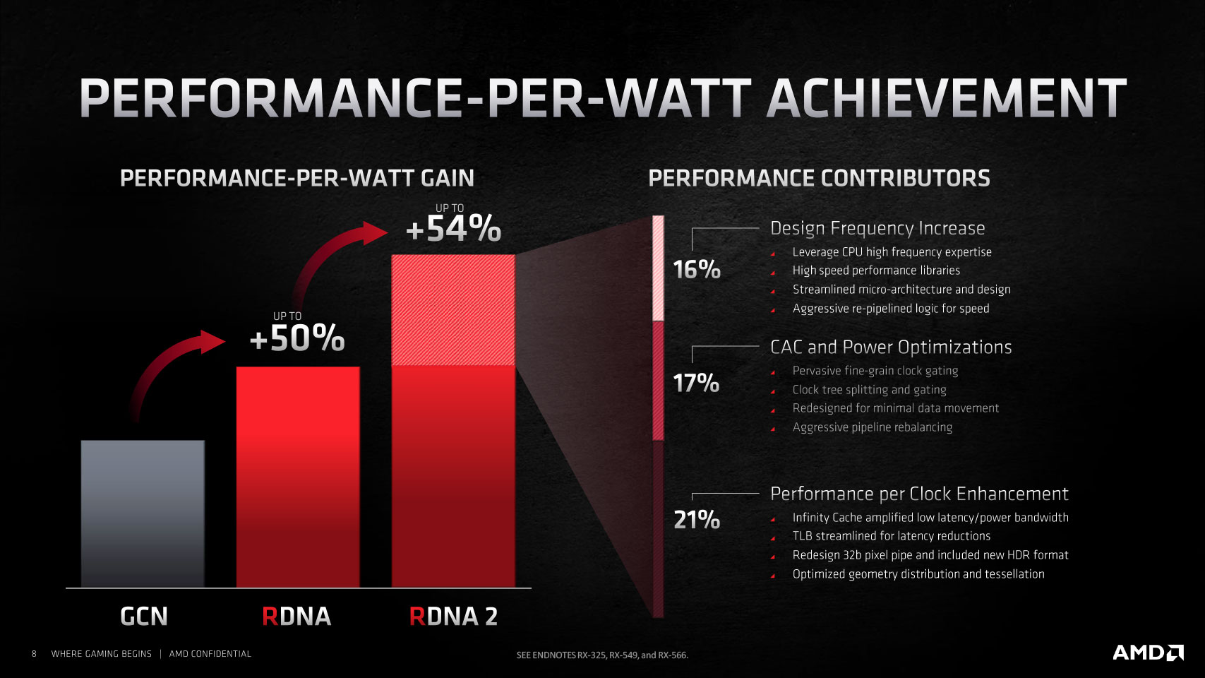
New design methodologies and component-level optimization throughout the silicon along with new power-management features allowed AMD to achieve two breakthroughs that enabled double the compute unit counts over the previous generation while staying within a reasonable power envelope. Firstly, the company managed to halve the power draw per CU while adding a 30% increase in engine clocks, which can both be redeemed for performance gain per CU.


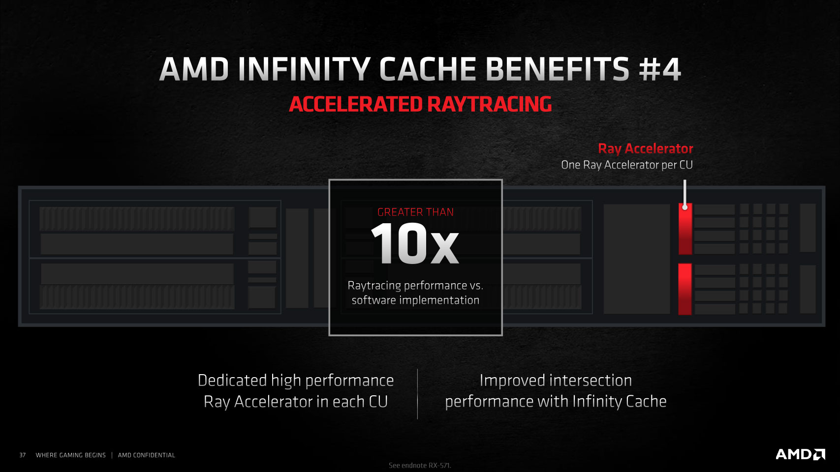
The RDNA2 compute unit is where a bulk of the magic happens. Arranged in groups of two called Dual Compute Units, which share instruction and data caches, the RDNA2 compute unit still packs 64 stream processors (128 per Dual CU) and has been optimized for increased frequencies, new kinds of math precision, new hardware that enables the Sampler Feedback feature, and the all-important Ray Accelerator, a fixed-function hardware component that calculates up to one triangle or four box ray intersections per clock cycle. AMD claims the Ray Accelerator makes intersection performance up to ten times faster than if it were executed with compute shaders. AMD also redesigned the render backends of the GPU from the ground up, towards enabling features such as Variable Rate Shading (both tier 1 and tier 2). At 64, the ROP count remains the same as for the previous-generation Navi 10.
Overall, the Navi 22 silicon has essentially the same component hierarchy as Navi 10. The Infinity Fabric interconnect is the link that binds all the components together. At the outermost level, you have the chip's 192-bit GDDR6 memory controllers, a PCI-Express 4.0 x16 host interface, and the multimedia and display engines which have been substantially updated from RDNA. A notch inside is the chip's 96-megabyte Infinity Cache, which we detail below. This cache is the town square for the GPU's high-speed 4 MB L2 caches and the graphics command processor, which dispatches the workload among two shader engines. Each of these shader engines packs 10 RDNA2 Dual Compute Units (or 20 CUs) along with the updated render backends and L1 cache. Combined, the silicon has 2,560 stream processors across 40 CUs, 40 Ray Accelerators (1 per CU), 160 TMUs, and 64 ROPs. In every sense except the memory, the Navi 22 is half a Navi 21.
The Radeon RX 6700 XT maxes out the Navi 22 silicon by enabling all 40 RDNA2 compute units. The card comes with 12 GB of GDDR6 memory running at 16 Gbps (GDDR6-effective) across the chip's 192-bit wide memory interface, which works out to 384 GB/s of memory bandwidth. The Infinity Cache runs at the highest possible 1.5 TB/s data-rate, while AMD claims that the engine clock can spike well above 2.50 GHz, with a 2.42 GHz "game clock."
Infinity Cache, or How AMD is Blunting NVIDIA's G6X Advantage


Despite its lofty design goals and a generational doubling in memory size to 12 GB, the RX 6700 XT has a rather unimpressive memory setup compared to NVIDIA's RTX 3070, or even AMD's own previous-generation RX 5700 XT. That is, at least on paper, with just a 192-bit bus width and JEDEC-standard 16 Gbps GDDR6, which works out to 384 GB/s raw bandwidth. Competing NVIDIA cards use 14 Gbps memory, but over a wider 256-bit memory interface. Memory compression secret sauce can at best increase effective bandwidth by a high single-digit percent.


AMD took a frugal approach to this problem, not wanting to invest in expensive HBM+interposer based solutions, which would have thrown overall production costs way off balance. AMD looked at how their Zen processor team leveraged large last-level caches on EPYC processors to significantly improve performance and carried the idea over to the GPU. A large chunk of the Navi 22 silicon die area now holds what AMD calls the "Infinite Cache," which is really just a new L3 cache that is 96 MB in size and talks to the GPU's four shader engines over a 1024 bit interface. This cache has an impressive bandwidth of 1.5 TB/s and can be used as a victim cache by the 4 MB L2 caches of the two shader engines.
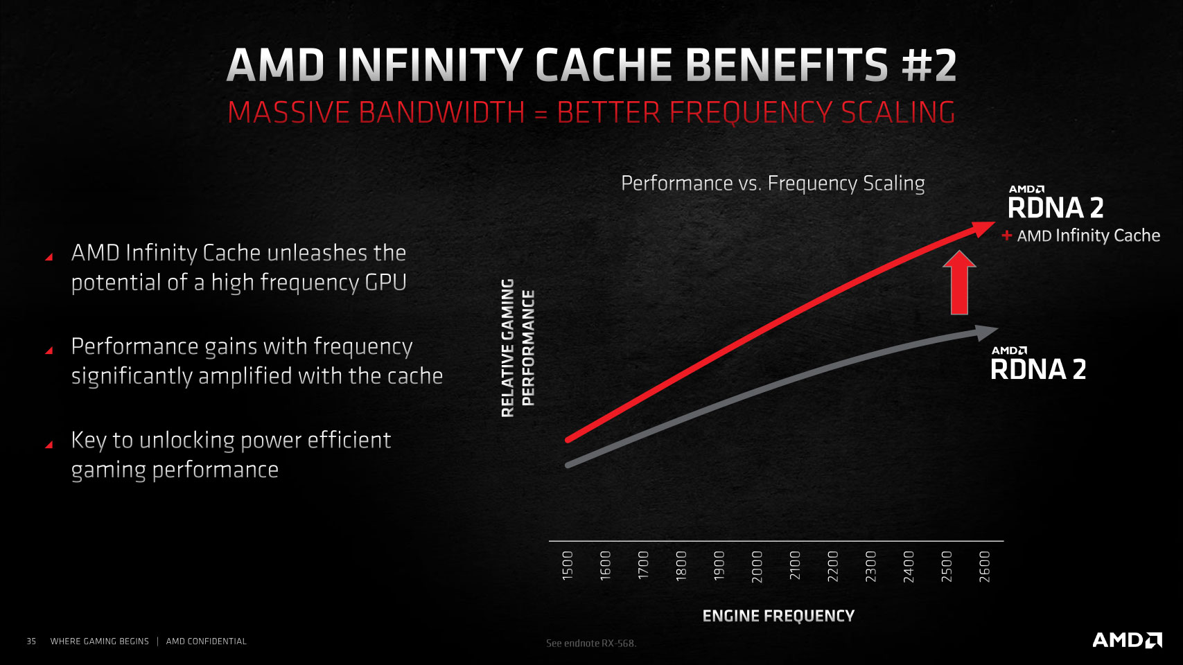

The physical media of Infinity Cache is the same class of SRAM as for the L3 cache on Zen processors. It offers four times the density of 4 MB L2 caches, lower bandwidth in comparison, but four times the bandwidth over GDDR6. It also significantly reduces energy consumption, by a sixth for the GPU to fetch a byte of data compared to doing so from GDDR6 memory. I'm sure the questions on your mind are what difference 96 MB makes and why no one has done this earlier.
To answer the first question, even with just 96 MB spread across two slabs of 48 MB each, Infinity Cache takes up a large amount of the die area of the Navi 22 silicon, and AMD's data has shown that much of the small workloads involved in raytracing and raster operations are bandwidth rather than memory-size intensive. Having a 96 MB fast victim cache running at extremely low latencies compared to DRAM helps. As for why AMD didn't do this earlier, it's only now that there's an alignment of circumstances where the company can afford to go with a fast 96 MB victim cache as opposed to just cramming in more CUs to get comparable levels of performance, but for less power consumption—as a storage rather than a logic device, spending die area on Infinity Cache instead of more CUs does result in power savings.
Apr 23rd, 2024 20:38 EDT
change timezone
Latest GPU Drivers
New Forum Posts
- What's your latest tech purchase? (20319)
- Post your Cinebench 2024 score (449)
- Sexy Mechanical Keyboard Thread (484)
- The TPU UK Clubhouse (24766)
- need help with motherboard/ ram compability certainty (14)
- My computer setup - Request for opinions (12)
- Show us your collections thread!! (282)
- Realtek Modded Audio Driver for Windows 10/11 - Only for HDAUDIO (5687)
- What phone you use as your daily driver? And, a discussion of them. (1454)
- Is there a technical reason that Windows 11 doesn't have built into it battery charge limitation? (37)
Popular Reviews
- Fractal Design Terra Review
- Corsair 2000D Airflow Review
- Thermalright Phantom Spirit 120 EVO Review
- Minisforum EliteMini UM780 XTX (AMD Ryzen 7 7840HS) Review
- ASUS GeForce RTX 4090 STRIX OC Review
- NVIDIA GeForce RTX 4090 Founders Edition Review - Impressive Performance
- ASUS GeForce RTX 4090 Matrix Platinum Review - The RTX 4090 Ti
- MSI GeForce RTX 4090 Gaming X Trio Review
- MSI GeForce RTX 4090 Suprim X Review
- Gigabyte GeForce RTX 4090 Gaming OC Review
Controversial News Posts
- Sony PlayStation 5 Pro Specifications Confirmed, Console Arrives Before Holidays (116)
- NVIDIA Points Intel Raptor Lake CPU Users to Get Help from Intel Amid System Instability Issues (106)
- AMD "Strix Halo" Zen 5 Mobile Processor Pictured: Chiplet-based, Uses 256-bit LPDDR5X (101)
- US Government Wants Nuclear Plants to Offload AI Data Center Expansion (98)
- Windows 10 Security Updates to Cost $61 After 2025, $427 by 2028 (84)
- Developers of Outpost Infinity Siege Recommend Underclocking i9-13900K and i9-14900K for Stability on Machines with RTX 4090 (84)
- TechPowerUp Hiring: Reviewers Wanted for Motherboards, Laptops, Gaming Handhelds and Prebuilt Desktops (74)
- Intel Realizes the Only Way to Save x86 is to Democratize it, Reopens x86 IP Licensing (70)