 99
99
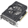
NVIDIA GeForce RTX 3050 6 GB Review - The Fastest Slot-Powered GPU
Test Setup »High-resolution PCB Pictures
These pictures are for the convenience of volt modders and people who would like to see all the finer details on the PCB. Feel free to link back to us and use these in your articles, videos or forum posts.

High-resolution versions are also available (front, back).
Circuit Board (PCB) Analysis


GPU voltage is an 3-phase design, managed by a Richtek RT8845A.

Sinopower SM4503+ SM4507 MOSFETs are used for GPU voltage; they are rated for 80 A of current each.

Memory voltage is a two-phase design, managed by a Richtek RT8237 (not pictured)

For memory, SM4507NH/4503NH are used, too.
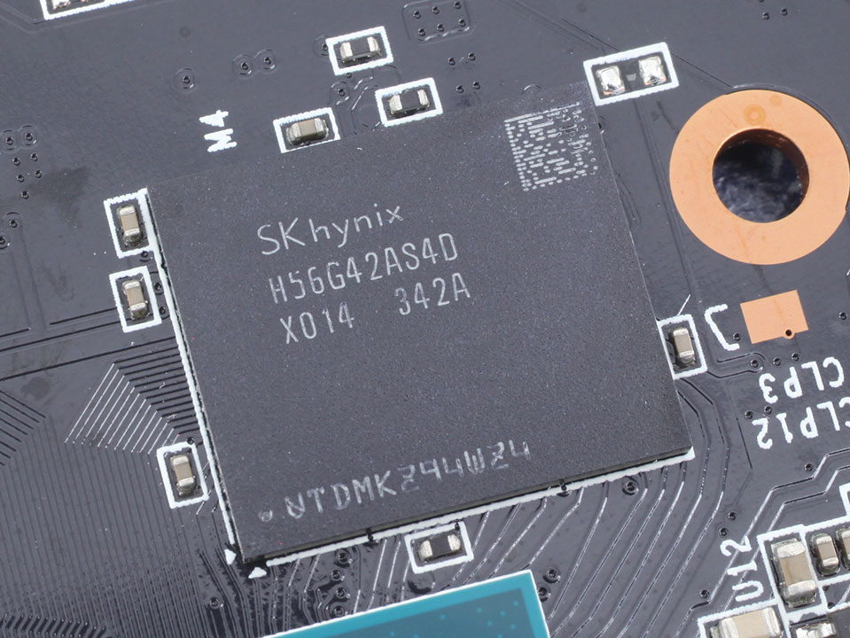
The GDDR6 memory chips are made by Hynix and carry the model number H56G42AS4DX014. They are specified to run at 2000 MHz (16 Gbps GDDR6 effective).
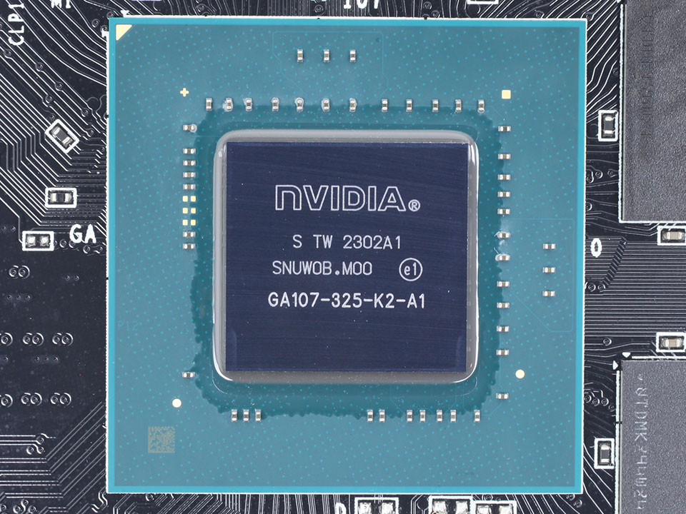
NVIDIA's GA107 graphics processor is built using a 8 nanometer process at Samsung, with a transistor count of 8.7 billion and a die size of 200 mm².
May 14th, 2024 20:33 EDT
change timezone
Latest GPU Drivers
New Forum Posts
- AMD RX 7000 series GPU Owners' Club (1105)
- Is it normal to hear this sound coming from the psu? (5)
- AM5 boot times improve RADICALLY with memory context restore enabled (51)
- Ryzen Owners Zen Garden (7333)
- What are you playing? (20649)
- Is It The 1080 TI The Best GPU Ever? (219)
- LOWER SSD PRICES (25)
- Purchased an AX1200i PSU as part of some forward planning, what tier is this PSU? (109)
- Free Games Thread (3805)
- 2024 and STILL no dark mode? (46)
Popular Reviews
- Homeworld 3 Performance Benchmark Review - 35 GPUs Tested
- Enermax REVOLUTION D.F. X 1200 W Review
- ZMF Caldera Closed Planar Magnetic Headphones Review
- Upcoming Hardware Launches 2023 (Updated Feb 2024)
- Corsair MP700 Pro SE 4 TB Review
- AMD Ryzen 7 7800X3D Review - The Best Gaming CPU
- ThundeRobot ML903 NearLink Review
- Bykski CPU-XPR-C-I CPU Water Block Review - Amazing Value!
- ASUS Radeon RX 7900 GRE TUF OC Review
- CHERRY XTRFY M64 Pro Review
Controversial News Posts
- Intel Statement on Stability Issues: "Motherboard Makers to Blame" (266)
- AMD to Redesign Ray Tracing Hardware on RDNA 4 (227)
- Windows 11 Now Officially Adware as Microsoft Embeds Ads in the Start Menu (172)
- NVIDIA to Only Launch the Flagship GeForce RTX 5090 in 2024, Rest of the Series in 2025 (152)
- AMD Hits Highest-Ever x86 CPU Market Share in Q1 2024 Across Desktop and Server (132)
- Sony PlayStation 5 Pro Specifications Confirmed, Console Arrives Before Holidays (119)
- AMD's RDNA 4 GPUs Could Stick with 18 Gbps GDDR6 Memory (114)
- AMD Ryzen 9 7900X3D Now at a Mouth-watering $329 (104)