 203
203
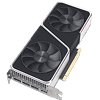
NVIDIA GeForce RTX 3060 Ti Founders Edition Review
(203 Comments) »Introduction
NVIDIA today released the GeForce RTX 3060 Ti, its fourth gaming graphics card based on their latest Ampere graphics architecture, targeting a wider market with its reduced price point. The RTX 3060 Ti debuts at a starting price of $400 and logically succeeds the RTX 2060 Super from the previous generation, which too launched at this price. We have with us for review the NVIDIA GeForce RTX 3060 Ti Founders Edition graphics card. NVIDIA designed the RTX 3060 Ti to offer smooth AAA gaming at the 1440p resolution, with additional horsepower for RTX raytracing. It should also serve as a gateway to 4K UHD resolution without raytracing or DLSS enabled, and should cater to the e-sports crowd, offering 1080p gaming at higher refresh rates, such as 144 Hz.
The GeForce RTX 3060 Ti is based on the same 8 nm "GA104" silicon as the RTX 3070, but with less of the shaders on the silicon enabled. It still ends up with more than double the number of CUDA cores as the RTX 2060 Super. NVIDIA claims that the RTX 3060 Ti is faster than the previous-generation RTX 2080 Super, which is a $700 high-end graphics card that fits the bill for 1440p + raytracing. All this is made possible because of the design goal with "Ampere"—to make RTX-on gameplay as fast as RTX-off gameplay on previous-generation cards given RTX raytracing remains an extremely compute-intensive technology that impacts performance in a big way. The obvious dividend of this approach would be a significant boost in non-raytraced (purely raster 3D) performance.

NVIDIA's GeForce Ampere graphics architecture marks the introduction of the 2nd generation RTX real-time raytracing technology. Pure raytraced 3D graphics may still be outside our reach, but it's possible to combine traditional raster 3D graphics with certain real-time raytraced elements, such as lighting, shadows, reflections, and global illumination. Even this much takes an enormous amount of compute power, and so NVIDIA innovated fixed-function hardware we will detail on the next page. The 2nd generation RTX combines new "Ampere" CUDA cores that offer concurrent FP32+INT32 math operations, with 2nd generation RT cores, which offer higher BVH traversal and intersection performance and new hardware that enabled raytraced motion blur; and the new 3rd generation Tensor core that leverages the sparsity phenomenon in deep-learning neural nets to improve AI inference performance by an order of magnitude over the previous generation.
NVIDIA carved the GeForce RTX 3060 Ti out of the "GA104" silicon by enabling 38 out of 48 streaming multiprocessors physically present on the silicon, resulting in 4,864 CUDA cores, 38 2nd generation RT cores, 152 3rd generation Tensor cores, 152 TMUs, and 80 ROPs. The CUDA core count has been increased by a staggering 123% over the RTX 2060 Super. The GPU clock speeds are roughly the same as those on the RTX 2060 Super, and yet typical board power isn't much higher with NVIDIA rating it at 200 W. This should mean that custom-design graphics cards with single 8-pin PCIe power connectors should be possible. The GPU is endowed with the same exact memory configuration as the RTX 3070: 8 GB of GDDR6 memory running at 14 Gbps across a 256-bit wide memory interface. This works out to 448 GB/s of bandwidth.
The NVIDIA GeForce RTX 3060 Ti Founders Edition is a beautiful rendition of the RTX 3060 Ti by its makers. The Founders Edition series of graphics cards by NVIDIA aren't exactly meant to serve as a baseline for the company's add-in card (AIC) partners to build on, but rather sets a high benchmark in product design for board partners to aspire to reach or beat. The RTX 3060 Ti Founders Edition looks almost identical in design to the RTX 3070 Founders Edition, but the color of the metal cooler frame differs slightly.
With its RTX 30-series Founders Edition cards, NVIDIA reduced the role of the cooler shroud to the frame, and lets exposed heatsinks make up most of the card's outer design. The card is longer than the PCB underneath, so airflow from the second fan flows unimpeded through the heatsink and out through a large vent on the backplate. The card uses the same 12-pin Molex MicroFit 3.0 power input as the other RTX 30-series FE cards, and an adapter is included to convert a single 8-pin PCIe input. In this review, we explore whether the RTX 3060 Ti is all you'll ever need if you're gaming at 1440p or below.
| Price | Shader Units | ROPs | Core Clock | Boost Clock | Memory Clock | GPU | Transistors | Memory | |
|---|---|---|---|---|---|---|---|---|---|
| RTX 2060 | $300 | 1920 | 48 | 1365 MHz | 1680 MHz | 1750 MHz | TU106 | 10800M | 6 GB, GDDR6, 192-bit |
| RX 5700 | $330 | 2304 | 64 | 1465 MHz | 1625 MHz | 1750 MHz | Navi 10 | 10300M | 8 GB, GDDR6, 256-bit |
| GTX 1080 | $330 | 2560 | 64 | 1607 MHz | 1733 MHz | 1251 MHz | GP104 | 7200M | 8 GB, GDDR5X, 256-bit |
| RTX 2060 Super | $380 | 2176 | 64 | 1470 MHz | 1650 MHz | 1750 MHz | TU106 | 10800M | 8 GB, GDDR6, 256-bit |
| RX Vega 64 | $400 | 4096 | 64 | 1247 MHz | 1546 MHz | 953 MHz | Vega 10 | 12500M | 8 GB, HBM2, 2048-bit |
| GTX 1080 Ti | $650 | 3584 | 88 | 1481 MHz | 1582 MHz | 1376 MHz | GP102 | 12000M | 11 GB, GDDR5X, 352-bit |
| RX 5700 XT | $370 | 2560 | 64 | 1605 MHz | 1755 MHz | 1750 MHz | Navi 10 | 10300M | 8 GB, GDDR6, 256-bit |
| RTX 2070 | $340 | 2304 | 64 | 1410 MHz | 1620 MHz | 1750 MHz | TU106 | 10800M | 8 GB, GDDR6, 256-bit |
| RTX 2070 Super | $450 | 2560 | 64 | 1605 MHz | 1770 MHz | 1750 MHz | TU104 | 13600M | 8 GB, GDDR6, 256-bit |
| Radeon VII | $680 | 3840 | 64 | 1802 MHz | N/A | 1000 MHz | Vega 20 | 13230M | 16 GB, HBM2, 4096-bit |
| RTX 2080 | $600 | 2944 | 64 | 1515 MHz | 1710 MHz | 1750 MHz | TU104 | 13600M | 8 GB, GDDR6, 256-bit |
| RTX 2080 Super | $690 | 3072 | 64 | 1650 MHz | 1815 MHz | 1940 MHz | TU104 | 13600M | 8 GB, GDDR6, 256-bit |
| RTX 3060 Ti | $400 | 4864 | 80 | 1410 MHz | 1665 MHz | 1750 MHz | GA104 | 17400M | 8 GB, GDDR6, 256-bit |
| RTX 2080 Ti | $1000 | 4352 | 88 | 1350 MHz | 1545 MHz | 1750 MHz | TU102 | 18600M | 11 GB, GDDR6, 352-bit |
| RTX 3070 | $500 | 5888 | 96 | 1500 MHz | 1725 MHz | 1750 MHz | GA104 | 17400M | 8 GB, GDDR6, 256-bit |
| RX 6800 | $580 | 3840 | 96 | 1815 MHz | 2105 MHz | 2000 MHz | Navi 21 | 23000M | 16 GB, GDDR6, 256-bit |
| RX 6800 XT | $650 | 4608 | 128 | 2015 MHz | 2250 MHz | 2000 MHz | Navi 21 | 23000M | 16 GB, GDDR6, 256-bit |
| RTX 3080 | $700 | 8704 | 96 | 1440 MHz | 1710 MHz | 1188 MHz | GA102 | 28000M | 10 GB, GDDR6X, 320-bit |
The GeForce Ampere Architecture
Earlier this year, on September 5, we published a comprehensive article on the NVIDIA GeForce Ampere graphics architecture, along with a deep-dive into the key 2nd Gen RTX technology and various other features NVIDIA is introducing that are relevant to gaming. Be sure to check out that article for more details.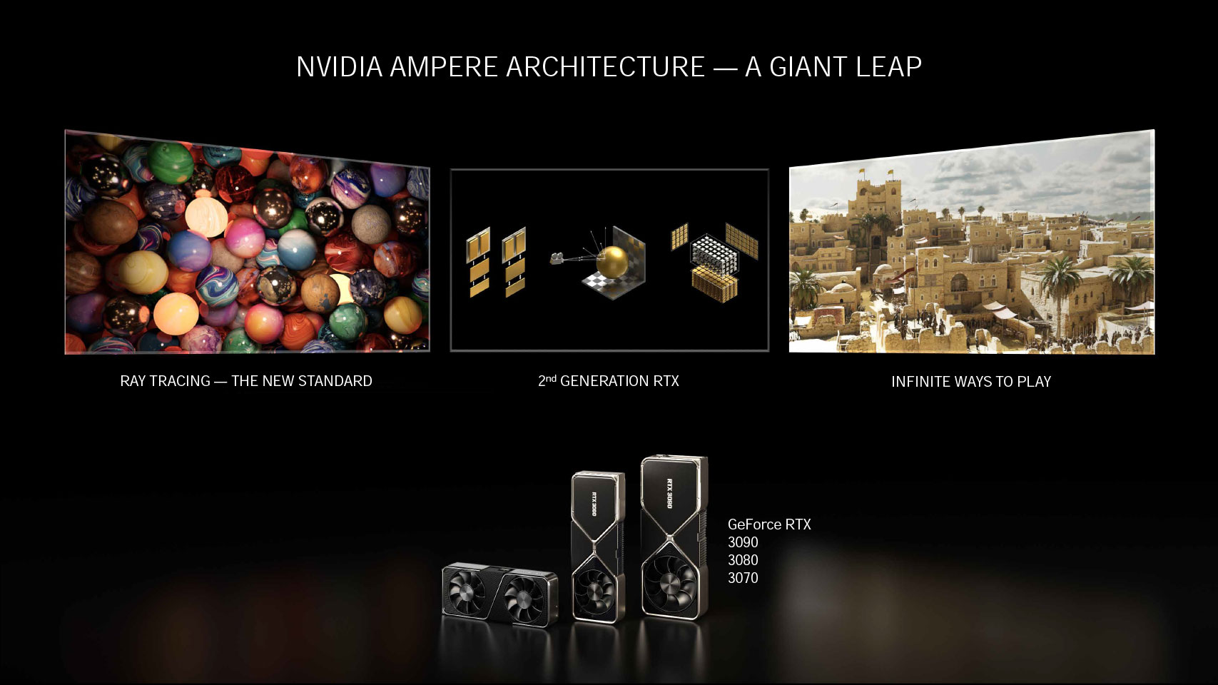
The GeForce Ampere architecture is the first time NVIDIA both converged and diverged its architecture IP between graphics and compute processors. Back in May, NVIDIA debuted Ampere on its A100 Tensor Core compute processor targeted at AI and HPC markets. The A100 Tensor Core is a headless compute chip that lacks all raster graphics components, so NVIDIA could cram in the things relevant to the segment. The GeForce Ampere, however, is a divergence with a redesigned streaming multiprocessor different from that of the A100. These chips have all the raster graphics hardware, display and media acceleration engines, and, most importantly, the 2nd generation RT core that accelerates real-time raytracing. A slightly slimmed down version of the 3rd generation tensor core of the A100 also gets carried over. NVIDIA sticks to using GDDR-type memory over expensive memory architectures, such as HBM2E.
NVIDIA pioneered real-time raytracing on consumer graphics hardware, and three key components make the NVIDIA RTX technology work: the SIMD components, aka CUDA cores, RT cores, which do the heavy lifting with raytracing, calculating BVH traversal and intersections, and tensor cores, which are hardware components accelerating AI deep-learning neural-net building and training. NVIDIA uses an AI-based denoiser for RTX. With Ampere, NVIDIA is introducing new generations of the three components, with the objective of reducing the performance cost of RTX and nearly doubling performance over generations. These include the new Ampere streaming multiprocessor that more than doubles FP32 throughput over generations, the 2nd Gen RT core that features hardware that enables new RTX effects, such as raytraced motion blur, and the 3rd generation tensor core, which leverages sparsity in DNNs to increase AI inference performance by an order of magnitude.
GA104 GPU and Ampere SM


The GeForce RTX 3060 Ti is the second graphics card to implement the company's GA104 Ampere silicon, which is the second largest chip based on the GeForce Ampere graphics architecture. NVIDIA shares the GA104 silicon between the RTX 3060 Ti and recently launched RTX 3070. The new GA104 chip is built on the same 8 nm silicon fabrication process by Samsung as the GA102. Its die crams in 17.4 billion transistors, a figure which is only slightly short of the 18.6 billion of the previous-generation flagship TU102, but over 10 billion short of the GA102. The die-area of the GA104 measures 392.5 mm².
The GA104 silicon features a largely similar component hierarchy to past-generation NVIDIA GPUs, but with the bulk of engineering effort focused on the new Ampere Streaming Multiprocessor (SM). The GPU supports the PCI-Express 4.0 x16 host interface, which doubles the host interface bandwidth over PCI-Express 3.0 x16. Also, unlike the GA102, the GA104 loses out on the blazing fast GDDR6X memory standard. It features the same 256-bit wide memory interface driving conventional GDDR6.
The GA104 silicon features six graphics processing clusters (GPCs), the mostly independent subunits of the GPU. Each GPC has four texture processing clusters (TPCs), the indivisible subunit that is the main number-crunching muscle of the GPU (unlike six TPCs per GPC on the GA102). Each TPC shares a PolyMorph engine between two streaming multiprocessors (SMs). The SM is what defines the generation and where the majority of NVIDIA's engineering effort is localized. The Ampere SM crams in 128 CUDA cores, double that of the 64 CUDA cores in the Turing SM. NVIDIA carved the RTX 3060 Ti out of the silicon by disabling 5 out of 24 TPCs. From the ROP count, we can infer that NVIDIA disabled an entire GPC with four TPCs, and a fifth TPC from any of the remaining GPCs.
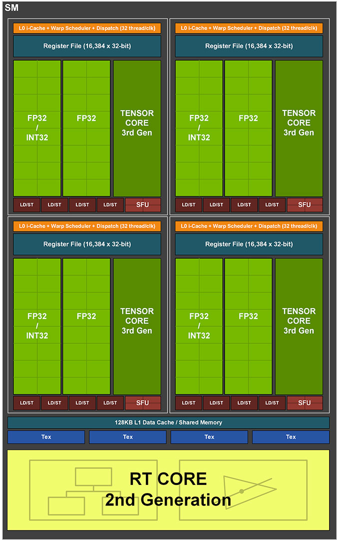

Each GeForce Ampere SM features four processing blocks that each share an L1I cache, warp scheduler, and a register file among 128 CUDA cores. From these, 64 can handle concurrent FP32 and INT32 math operations, while 64 are pure FP32. Each cluster also features a 3rd generation Tensor Core. At the SM level, the four processing blocks share a 128 KB L1D cache that also serves as shared memory; four TMUs and a 2nd generation RT core. As we mentioned, each processing block features two FP32 data paths; one of these consists of CUDA cores that can execute 16 FP32 operations per clock cycle, while the other data path consists of CUDA cores capable of 16 FP32 and 16 INT32 concurrent operations per clock. Each SM also features a tiny, unspecified number of rudimentary FP64 cores, which work at 1/64 the performance of the FP64 cores on the A100 Tensor Core HPC processor. These FP64 cores are only there so double-precision software doesn't run into compatibility problems.
2nd Gen RT Core, 3rd Gen Tensor Core


NVIDIA's 2nd generation RTX real-time raytracing technology sees the introduction of more kinds of raytraced effects. NVIDIA's pioneering technology involves composing traditional raster 3D scenes with certain raytraced elements, such as lighting, shadows, global illumination, and reflections.


As explained in the Ampere Architecture article, NVIDIA's raytracing philosophy involves heavy bounding volume hierarchy (BVH) traversal, and bounding box/triangle intersection, for which NVIDIA developed a specialized MIMD fixed function in the RT core. Fixed-function hardware handles both the traversal and intersection of rays with bounding boxes or triangles. With the 2nd Gen RT core, NVIDIA is introducing a new component which interpolates triangle position by time. This component enables physically accurate, raytraced motion-blur. Until now, motion-blur was handled as a post-processing effect.


The 3rd generation tensor core sees NVIDIA build on the bulwark of its AI performance leadership, fixed-function hardware designed for tensor math which accelerates AI deep-learning neural-net building and training. AI is heavily leveraged in NVIDIA architectures now, as the company uses an AI-based denoiser for its raytracing architecture and to accelerate technologies such as DLSS. Much like the 3rd generation tensor cores on the company's A100 Tensor Core processor that debuted this Spring, the new tensor cores leverage a phenomenon called sparsity—the ability for a DNN to shed its neural net without losing the integrity of its matrix. Think of this like Jenga: you pull pieces from the middle of a column while the column itself stays intact. The use of sparsity increases AI inference performance by an order of magnitude: 256 FP16 FMA operations in a sparse matrix compared to just 64 on the Turing tensor core, and 1024 sparse FP16 FMA ops per SM compared to 512 on the Turing SM, which has double the tensor core counts.
Display and Media

NVIDIA updated the display and media acceleration components of Ampere. To begin with, VirtualLink, or the USB type-C connection, has been removed from the reference design. We've seen no other custom-design cards implement it, so it's safe to assume NVIDIA junked it. The GeForce RTX 3080 puts out three DisplayPort 1.4a, which takes advantage of the new VESA DSC 1.2a compression technology to enable 8K 60 Hz with HDR using a single cable. It also enables 4K at 240 Hz with HDR. The other big development is support for HDMI 2.1, which enables 8K at 60 Hz with HDR, using the same DSC 1.2a codec. NVIDIA claims that DSC 1.2a is "virtually lossless" in quality. The media acceleration features are largely carried over from Turing, except for the addition of AV1 codec hardware decode. As the next major codec to be deployed by the likes of YouTube and Netflix, AV1 is big. It halves the file size over H.265 HEVC for comparable quality. The new H.266 standard misses out as it was introduced too late during Ampere's development.
NVIDIA Ampere Features
Hardware architecture only paints half the story of what's new with GeForce Ampere. Here, we quickly run you through the noteworthy new features introduced by the GeForce RTX 30 series. Some of these will work even with the RTX 20 series through driver updates. When NVIDIA introduced the RTX 20 series Turing, the hot new feature was RTX and real-time raytracing, along with AI acceleration. NVIDIA builds on these with its 2nd generation RTX architecture for vast generational performance improvements. NVIDIA is so confident in the performance uplift that it set its eyes on 8K gameplay. This was probably important as new-generation game consoles, such as the PlayStation 5 and Xbox Series X, formally advertise 4K gaming. High-end gaming PCs can't be seen to play in the same field.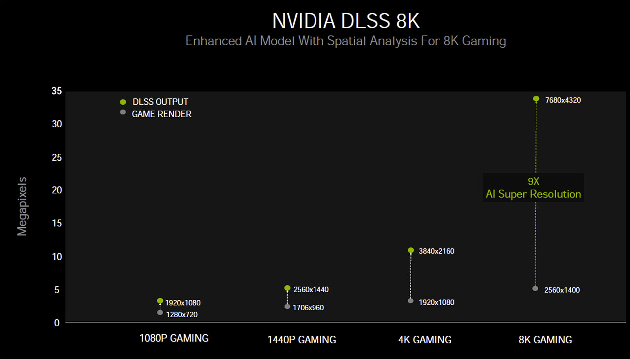
8K is four times the pixels of 4K, or sixteen times Full HD, which is no small ask. Yet NVIDIA believes it can take a crack at 8K by using the new 8K DLSS feature in combination with its new display outputs that support 8K 60 Hz leveraging DSC 1.2a. 8K DLSS renders the game at 1440p and uses a special 9X Super Sampling algorithm to reconstruct details at 8K. NVIDIA demonstrated that this looks better than merely running the game at 8K and making it scale up game assets using bilinear upscaling. The company also listed a large selection of games where frame rates above 8K were obtained.
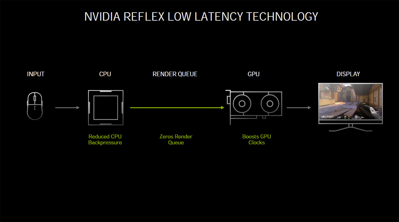

With competitive e-sports gaming that has millions riding on it, it's not enough that network latency is reduced and frame rates increased. NVIDIA discovered that "whole system latency" plays an equally important role as network latency in affecting gamers' competitiveness. System latency is defined by NVIDIA as the time it takes for you to physically click a button on your mouse and for the click to register in-game as an action. In the heat of gameplay, system latency can mean the difference between scoring a hit against the opponent or their getting away. NVIDIA Reflex is a feature that works to minimize system latency.
On the software side, the NVIDIA driver co-operates with a compatible game engine to optimize the game's 3D rendering pipeline. This is accomplished by dynamically reducing the rendering queue, so fewer frames are queued up for the GPU to render. NVIDIA claims that the technology can also keep the GPU perfectly in sync with the CPU, reducing the "back-pressure" on the GPU by letting the game sample mouse input at the last possible moment. NVIDIA is releasing Reflex to gamers as GeForce driver updates, and to game developers as the Reflex SDK. This allows them to integrate the technology into their game engine with a toggle for the technology, and also put out in-game performance metrics.


Although NVIDIA Reflex works with any monitor, the company also introduced a new display standard targeted at competitive e-sports gamers it dubbed the "NVIDIA G-SYNC 360 e-Sports Display." This is a display feature-set logo that certifies a monitor as featuring an IPS dual-driver panel with a 360 Hz refresh rate, at least 240 Hz ultra-low motion blur (ULMB), the new G-SYNC e-sports mode, and hardware support for the NVIDIA Reflex Latency Analyzer feature. On these displays, you'll find an integrated 2-port USB hub. You plug this hub into your PC via an included USB cable and plug your gaming mouse into one of two downstream USB ports on the monitor. This can be any mouse, but an NVIDIA-certified mouse (ASUS, Razer, or Logitech) will offer additional features.
With the mouse plugged in, you launch the Reflex Latency Analyzer utility from the monitor's OSD settings and run the game with the Reflex metrics toggle enabled. Each time you click on the mouse, the click is registered in the USB hub of the monitor, which then measures the time it takes for the "output" gun flash pixels to appear on screen. You can train the utility to look for where the gun muzzle flash pixels appear. This way, you get extremely accurate measurements of not just input latency, but also end-to-end system latency. Something like this required high-speed cameras and manual math to calculate in the past. Input latencies, coupled with end-to-end latency data, can be viewed in the Performance Metrics screen of the GeForce Experience overlay, when spawned in a compatible game.


Storage has traditionally been the slowest component in the PC, which also happens to have the highest overhead (associated with IO, data compression, and in some cases encryption). With the introduction of NVMe, SSD sequential transfer rates are on a meteoric rise, as is storage IO overhead. NVIDIA predicts that for a 7 GB/s NVMe SSD that takes advantage of PCIe Gen 4, which is moving compressed data to the GPU, the overhead could have a tangible impact on CPU performance, saturating as many as 24 logical processors. NVIDIA RTX-IO aims to fix this by leveraging the Microsoft DirectStorage API with NVIDIA-specific optimizations on top. RTX-IO enables compressed data transfers between your SSD and the GPU memory with minimal involvement of the CPU. The compressed data stream is decompressed by the GPU's compute capability. RTX-IO requires game-level support. Since most games for next-gen consoles have some sort of readiness for DirectStorage, RTX-IO support won't be too far behind.

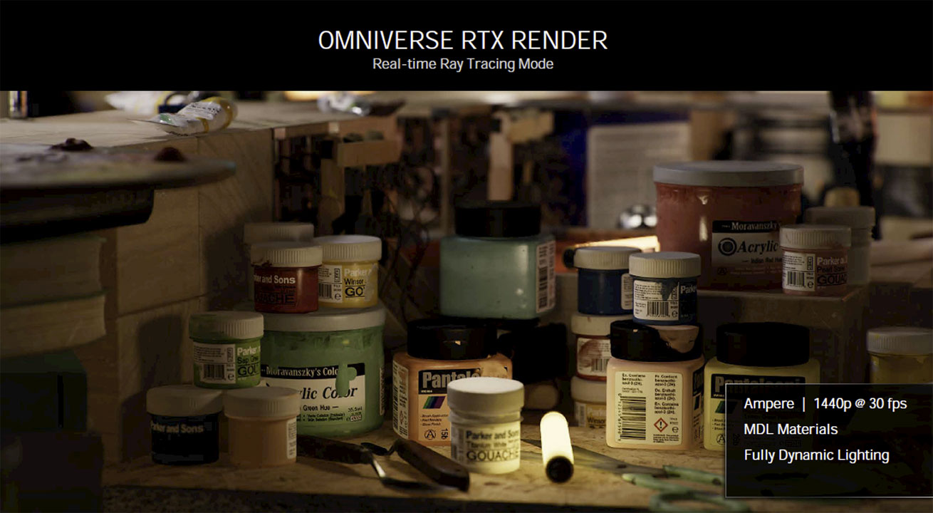
When NVIDIA introduced Ansel a few years ago, it spawned a new class of still art using in-game assets. What if you could make 3D animated movies using in-game assets? This concept is called machinima and already has a small, growing community of artists. NVIDIA wants to democratize and grow this ecosystem by introducing the new Omniverse Machinima software. When used with a supporting game, the software lets you make detailed 3D movies using all available game assets—think making your own Star Trek fan fiction using STO assets.
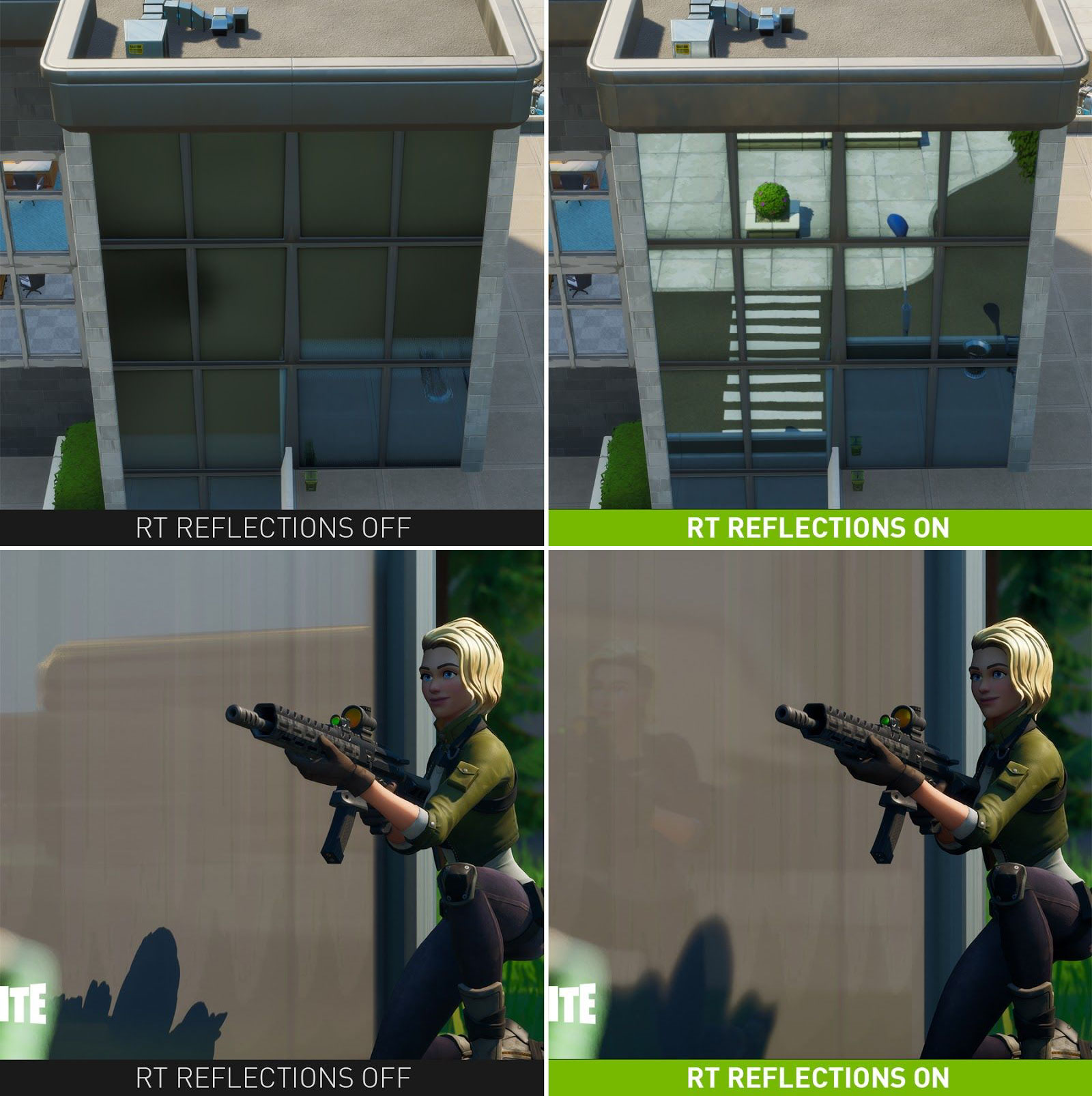
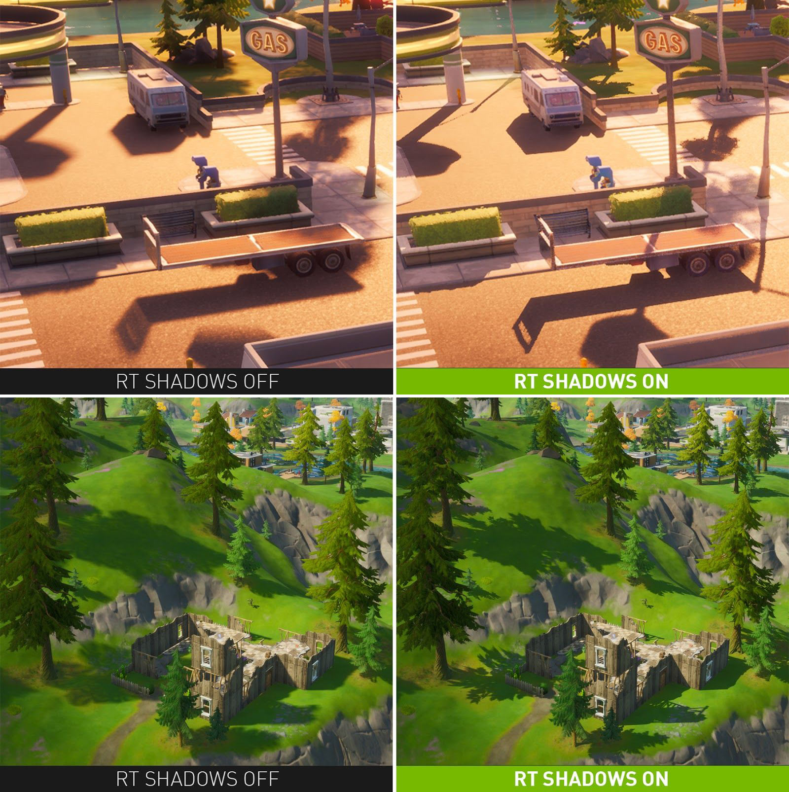

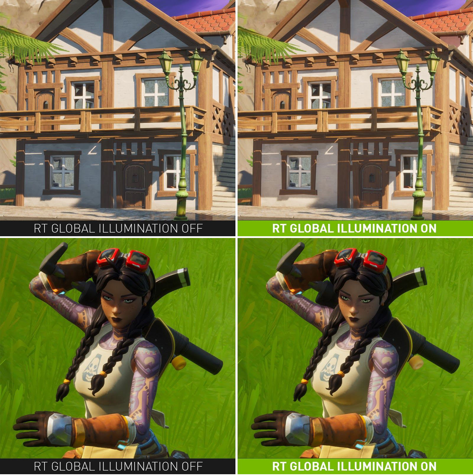
When you think about RTX, it's often AAA games that come to mind, and not competitive e-sports titles, as RTX inflicts a performance costs and e-sports titles are designed to favor performance over eye candy. This is about to change with Fortnite going RTX-on. Fortnite uses almost the entire RTX feature set, including raytraced reflections, shadows, ambient occlusion, and global illumination. The game also implements DLSS, letting it render at a lower resolution, and uses AI supersampling to restore details. Epic claims that DLSS at 4K looks better than even native 4K rendering.
Our Patreon Silver Supporters can read articles in single-page format.
Aug 1st, 2025 15:49 CDT
change timezone
Latest GPU Drivers
New Forum Posts
- Samsung 870 EVO - Beware, certain batches prone to failure! (1302)
- AMD Radeon 6900 XT Limited Black Edition Bios Problems - Boost Problems (9)
- Have you got pie today? (16818)
- WCG Daily Numbers (12955)
- What are you playing? (24029)
- Blender 4.0.1 BMW27 demo test (22)
- Can't find vbios for Rx 470 (6)
- TPU's Rosetta Milestones and Daily Pie Thread (2419)
- Folding Pie and Milestones!! (9661)
- 3DMARK "LEGENDARY" (357)
Popular Reviews
- MSI Claw 8 AI+ A2VM Review
- Lenovo Legion 5i (15IRX10) Review - Feature-Rich and Wallet Friendly
- ASUS ROG Crosshair X870E Apex Review
- Herman Miller Logitech G Embody Review - No Pain, No Gain
- Orbital Pathfinder Review
- Montech X5 Review
- Upcoming Hardware Launches 2025 (Updated May 2025)
- Lian Li O11 Dynamic Mini V2 Review
- Noctua NF-A12x25 G2 PWM Fan Review
- AMD Ryzen 7 9800X3D Review - The Best Gaming Processor
TPU on YouTube
Controversial News Posts
- AMD's Upcoming UDNA / RDNA 5 GPU Could Feature 96 CUs and 384-bit Memory Bus (137)
- AMD Radeon RX 9070 XT Gains 9% Performance at 1440p with Latest Driver, Beats RTX 5070 Ti (131)
- Intel "Nova Lake-S" Core Ultra 3, Ultra 5, Ultra 7, and Ultra 9 Core Configurations Surface (110)
- DDR6 Memory Arrives in 2027 with 8,800-17,600 MT/s Speeds (102)
- NVIDIA to Debut GeForce RTX 50-series SUPER GPUs by Christmas (101)
- AMD Sampling Next-Gen Ryzen Desktop "Medusa Ridge," Sees Incremental IPC Upgrade, New cIOD (97)
- Intel CEO Confirms SMT To Return to Future CPUs (95)
- NVIDIA Becomes First Company Ever to Hit $4 Trillion Market-Cap (94)