 355
355
NVIDIA GeForce RTX 3080 Founders Edition Review - Must-Have for 4K Gamers
Ampere Features »The GeForce Ampere Architecture
Earlier this month, on September 5, we did a comprehensive article on the NVIDIA GeForce Ampere graphics architecture, along with a deep-dive into the key 2nd Gen RTX technology and various other features NVIDIA is introducing that are relevant to gaming. Be sure to check out that article for more details.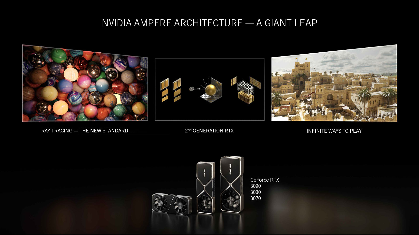

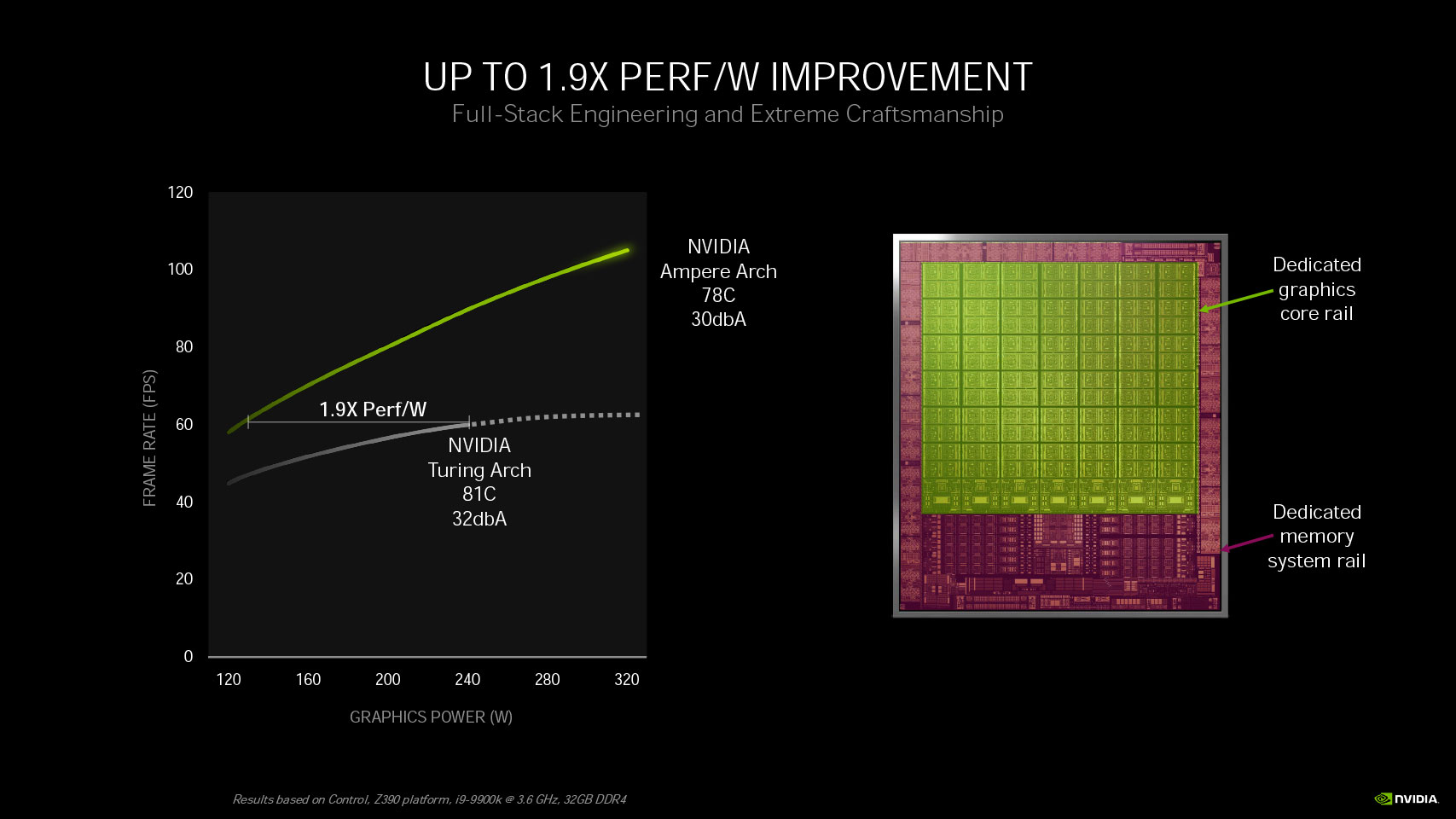
The GeForce Ampere architecture is the first time NVIDIA both converged and diverged its architecture IP between graphics and compute processors. Back in May, NVIDIA debuted Ampere on its A100 Tensor Core compute processor targeted at AI and HPC markets. The A100 Tensor Core is a headless compute chip that lacks all raster graphics components, so NVIDIA could cram in the things relevant to the segment. The GeForce Ampere, however, is a divergence, with a redesigned streaming multiprocessor different from that of the A100. These chips have all the raster graphics hardware, display and media acceleration engines, and, most importantly, the 2nd generation RT core that accelerates real-time raytracing. A slightly slimmed down version of the 3rd generation tensor core of the A100 also gets carried over. NVIDIA sticks to using GDDR-type memory over expensive memory architectures, such as HBM2E. Memory sizes have been increased generation over generation, as well as memory bus widths, but NVIDIA also worked with Micron Technology to introduce a new non-JEDEC memory type it calls GDDR6X, which increases data rates by over 20 percent over GDDR6.
NVIDIA pioneered real-time raytracing on consumer graphics hardware, and three key components make the NVIDIA RTX technology work: the SIMD components, aka CUDA cores, the RT cores, which do the heavy lifting with raytracing, calculating BVH traversal, and intersections, and tensor cores, which are hardware component accelerating AI deep-learning neural net building, and training. NVIDIA uses an AI-based denoiser for RTX. With Ampere, NVIDIA is introducing new generations of the three components, with the objective being to reduce the performance cost of RTX, and nearly double performance over generations. These include the new Ampere streaming multiprocessor that more than doubles FP32 throughput over generations, the 2nd Gen RT core that features hardware that enables new RTX effects, such as raytraced motion blur, and the 3rd generation tensor core, which leverages sparsity in DNNs to increase AI inference performance by an order of magnitude.
GA102 GPU and Ampere SM

NVIDIA is taking a new approach to segmenting its high-end graphics cards with this generation. While the RTX 2080 and RTX 2080 Ti from the past generation were based on two different pieces of silicon—the TU104 and TU102 respectively—the new RTX 3080 and upcoming RTX 3090 are based a common silicon, the GA102, which is the biggest based on the GeForce Ampere architecture. The GA102 is based on the new Samsung 8N silicon fabrication process, an 8 nm node Samsung specially designed for NVIDIA, offering comparable transistor densities and iso-power to TSMC's 7 nm-class nodes. This large 628.4 mm² piece of silicon crams in 28.3 billion transistors.
The GA102 silicon features a largely similar component hierarchy to past-generation NVIDIA GPUs, but with the bulk of engineering effort focused on the new Ampere Streaming Multiprocessor (SM). The GPU supports the PCI-Express 4.0 x16 host interface, which doubles the host interface bandwidth over PCI-Express 3.0 x16. In today's GeForce RTX 3080 PCI-Express Scaling article, we test whether the RTX 3080 can actually benefit from PCIe Gen 4. With this generation, NVIDIA is also relegating SLI and the NVLink interface to only the top-dog RTX 3090, even the RTX 3080 loses out on it. With the past generation, even the RTX 2070 Super had NVLink. The decision to use a common silicon between the RTX 3080 and RTX 3090 may have had a lot to do with the memory bandwidth target. The RTX 3080 is endowed with a 320-bit wide memory interface, which is wider than the 256-bit interface of the RTX 2080.
The GA102 silicon features seven graphics processing clusters (GPCs), the mostly independent subunits of the GPU, from which one GPC is completely disabled on the RTX 3080. Each GPC has six texture processing clusters (TPCs), the indivisible subunit that is the main number-crunching muscle of the GPU. In addition to a whole GPC, two random TPCs are disabled from the remaining six GPCs to carve out the RTX 3080. Each TPC shares a PolyMorph engine between two streaming multiprocessors (SMs). The SM is what defines the generation and where the majority of NVIDIA's engineering effort is localized. The Ampere SM crams in 128 CUDA cores, double that of the 64 CUDA cores in the Turing SM.
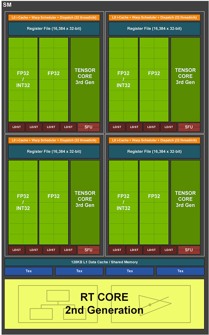

Each GeForce Ampere SM features four processing blocks that each share an L1I cache, warp scheduler, and a register file among 128 CUDA cores. From these, 64 can handle concurrent FP32 and INT32 math operations, while 64 are pure FP32. Each cluster also features a 3rd generation Tensor Core. At the SM level, the four processing blocks share a 128 KB L1D cache that also serves as shared memory; four TMUs and a 2nd generation RT core. As we mentioned, each processing block features two FP32 data paths; one of these consists of CUDA cores that can execute 16 FP32 operations per clock cycle, while the other data path consists of CUDA cores capable of 16 FP32 and 16 INT32 concurrent operations per clock. Each SM also features a tiny, unspecified number of rudimentary FP64 cores, which work at 1/64 the performance of the FP64 cores on the A100 Tensor Core HPC processor. These FP64 cores are only there so double-precision software doesn't run into compatibility problems.
2nd Gen RT Core, 3rd Gen Tensor Core


NVIDIA's 2nd generation RTX real-time raytracing technology sees the introduction of more kinds of raytraced effects. NVIDIA's pioneering technology involves composing traditional raster 3D scenes with certain raytraced elements, such as lighting, shadows, global illumination, and reflections.
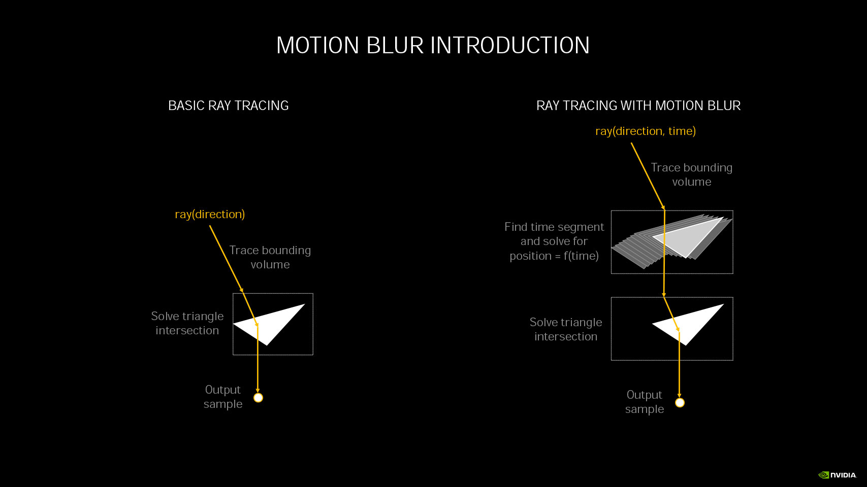

As explained in the Ampere Architecture article, NVIDIA's raytracing philosophy involves heavy bounding volume hierarchy (BVH) traversal, and bounding box/triangle intersection, for which NVIDIA developed specialized MIMD fixed function in the RT core. Fixed-function hardware handles both traversal and intersection of rays with bounding boxes or triangles. With the 2nd Gen RT core, NVIDIA is introducing a new component which interpolates triangle position by time. This component enables physically accurate, raytraced motion-blur. Until now, motion-blur was handled as a post-processing effect.

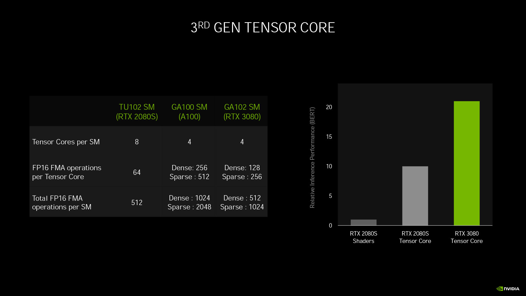
The 3rd generation tensor core sees NVIDIA build on the bulwark of its AI performance leadership, fixed-function hardware designed for tensor math, which accelerates AI deep-learning neural-net building and training. AI is heavily leveraged in NVIDIA architectures now, as the company uses an AI-based denoiser for its raytracing architecture, and to accelerate technologies such as DLSS. Much like the 3rd generation tensor cores on the company's A100 Tensor Core processor that debuted this Spring, the new tensor cores leverage a phenomenon called sparsity—the ability for a DNN to shed its neural net without losing the integrity of its matrix. Think of this like Jenga: you pull pieces from the middle of a column, while the column itself stays intact. The use of sparsity increases AI inference performance by an order of magnitude: 256 FP16 FMA operations in a sparse matrix compared to just 64 on the Turing tensor core, and 1024 sparse FP16 FMA ops per SM compared to 512 on the Turing SM (which has double the tensor core counts).
GDDR6X Memory
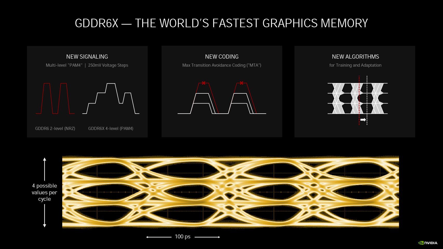
NVIDIA partnered with Micron Technology to develop a new exclusive memory technology for GeForce Ampere, which it calls GDDR6X. This isn't a JEDEC standard, but builds on GDDR6 with the implementation of the new PAM4 physical layer signaling technology, making it possible to transmit four possible values per clock cycle. PAM4 transmits at four different voltage levels to pack double the data per clock cycle. This enables data-rates nearing 20 Gbps, or close to 25% higher than what's possible with 16 Gbps GDDR6 memory available on the market today. The RTX 3080 is configured with 19 Gbps memory frequency, and the RTX 3090 takes it a notch higher with 19.5 Gbps. Over a 320-bit wide memory bus, this translates to 760 GB/s of bandwidth for the RTX 3080, a nearly 70% increase over that of the RTX 2080!
Of course, it wasn't an easy engineering feat for NVIDIA and Micron. Two new innovations were needed for GDDR6X to sustain its signal integrity. The new Max Transmission Avoidance coding scheme ensures that the four levels don't overlap with each other. The second innovation is a new memory controller that re-trains the memory from time to time in response to changes in the environment, such as ambient temperature or EM interference.
Display and Media
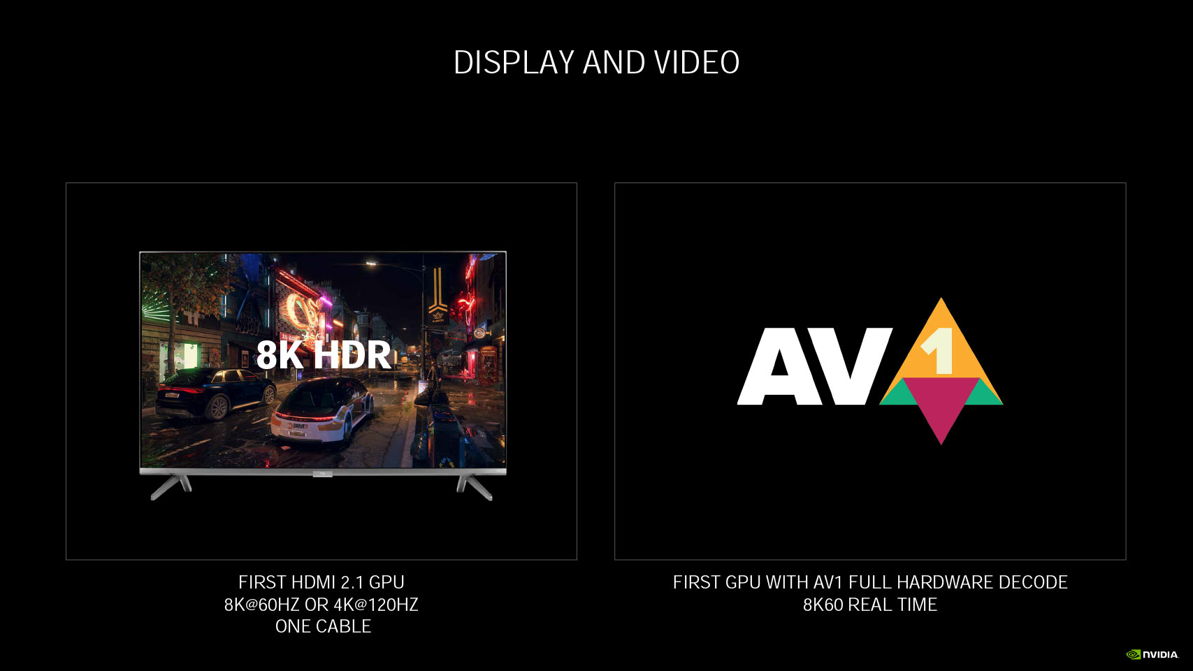
NVIDIA updated the display and media acceleration components of Ampere. To begin with, VirtualLink, or the USB type-C connection, has been removed from the reference design. We've seen no other custom-design cards implement it, so it's safe to assume NVIDIA junked it. The GeForce RTX 3080 puts out three DisplayPort 1.4a, which takes advantage of the new VESA DSC 1.2a compression technology to enable 8K 60 Hz with HDR using a single cable. It also enables 4K at 240 Hz with HDR. The other big development is support for HDMI 2.1, which enables 8K at 60 Hz with HDR, using the same DSC 1.2a codec. NVIDIA claims that DSC 1.2a is "virtually lossless" in quality. The media acceleration features are largely carried over from Turing, except for the addition of AV1 codec hardware decode. As the next big codec to be deployed by the likes of YouTube and Netflix, AV1 is big. It halves the file size over H.265 HEVC for comparable quality. The new H.266 VVC misses out as the standard was introduced too late into Ampere's development.
Apr 18th, 2024 19:16 EDT
change timezone
Latest GPU Drivers
New Forum Posts
- MSI Z790 owners - be careful, the screw can crack the chipset (3)
- WCG Daily Numbers (12489)
- TPU's Nostalgic Hardware Club (18448)
- TPU's Rosetta Milestones and Daily Pie Thread (1854)
- Last game you purchased? (251)
- Seeking Compatible VBIOS for RX 580 8GB (20)
- Folding Pie and Milestones!! (9001)
- EDP other basically constantly red while playing games (4)
- Is it possible that the atmosphere is losing less of its "shield" capabilities due to more and more jets/rockets puncturing it daily? (19)
- Will a RTX 4070 TI super bottleneck a Ryzen 9 7950X3D? (34)
Popular Reviews
- Horizon Forbidden West Performance Benchmark Review - 30 GPUs Tested
- PowerColor Radeon RX 7900 GRE Hellhound Review
- Fractal Design Terra Review
- Corsair 2000D Airflow Review
- Minisforum EliteMini UM780 XTX (AMD Ryzen 7 7840HS) Review
- Creative Pebble X Plus Review
- Thermalright Phantom Spirit 120 EVO Review
- FiiO KB3 HiFi Mechanical Keyboard Review - Integrated DAC/Amp!
- ASUS GeForce RTX 4090 STRIX OC Review
- NVIDIA GeForce RTX 4090 Founders Edition Review - Impressive Performance
Controversial News Posts
- Sony PlayStation 5 Pro Specifications Confirmed, Console Arrives Before Holidays (109)
- NVIDIA Points Intel Raptor Lake CPU Users to Get Help from Intel Amid System Instability Issues (102)
- US Government Wants Nuclear Plants to Offload AI Data Center Expansion (98)
- Windows 10 Security Updates to Cost $61 After 2025, $427 by 2028 (82)
- Developers of Outpost Infinity Siege Recommend Underclocking i9-13900K and i9-14900K for Stability on Machines with RTX 4090 (82)
- TechPowerUp Hiring: Reviewers Wanted for Motherboards, Laptops, Gaming Handhelds and Prebuilt Desktops (71)
- Intel Realizes the Only Way to Save x86 is to Democratize it, Reopens x86 IP Licensing (70)
- AMD Zen 5 Execution Engine Leaked, Features True 512-bit FPU (63)