 1
1
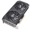
Palit GeForce RTX 4060 Ti Dual OC Review
Test Setup »High-resolution PCB Pictures
These pictures are for the convenience of volt modders and people who would like to see all the finer details on the PCB. Feel free to link back to us and use these in your articles, videos or forum posts.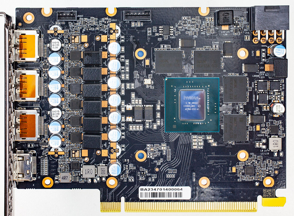

High-resolution versions are also available (front, back).
Circuit Board (PCB) Analysis
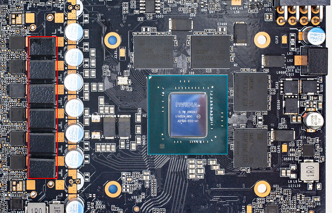

GPU voltage regulation is a 6-phase design, driven by a UPI uP9512R controller that's capable of handling up to 8 phases.

OnSemi NCP302150 DrMOS components are used for GPU voltage; they are rated for 50 A of current each.


Memory voltage is a single phase design, and handled by a 7212 buck controller.

For memory, Palit is using a set of Sinopower SM4377 and 4503NH series DPAK discrete MOSFETs, this set is rated for 50 A.

The memory chips are Samsung K4ZAF325BC-SC20, these are 20 Gbps-rated GDDR6 memory chips.

NVIDIA's AD106 graphics processor is the company's fourth Ada Lovelace GPU. It is built using a 5 nanometer process at TSMC Taiwan, with a transistor count of 22.9 billion and a die size of 190 mm².
May 9th, 2024 18:42 EDT
change timezone
Latest GPU Drivers
New Forum Posts
- Last game you purchased? (277)
- Keysfan (25)
- Microsoft butchering Xbox Studios (41)
- Flash VBIOS to turn RX 580 2048SP into RX 570 (25)
- not impressed - nvme vs ssd (75)
- Only some humans can see refresh rates faster than others, I am one of those humans. (237)
- Why does my PC shut down even though it's connected to a UPS? (85)
- looking to optimize (performance+cooling) a ryzen 7800x3d system with x670e aorus pro x (10)
- AM5 boot times improve RADICALLY with memory context restore enabled (14)
- 6800XT Red Devil with 18°C difference from Core to Hotspot (11)
Popular Reviews
- CHERRY XTRFY M64 Pro Review
- Corsair iCUE Link RX120 RGB 120 mm Fan Review
- Bykski CPU-XPR-C-I CPU Water Block Review - Amazing Value!
- Finalmouse UltralightX Review
- Upcoming Hardware Launches 2023 (Updated Feb 2024)
- Corsair MP700 Pro SE 4 TB Review
- AMD Ryzen 7 7800X3D Review - The Best Gaming CPU
- Cougar Hotrod Royal Gaming Chair Review
- ASUS Radeon RX 7900 GRE TUF OC Review
- Meze Audio LIRIC 2nd Generation Closed-Back Headphones Review
Controversial News Posts
- Intel Statement on Stability Issues: "Motherboard Makers to Blame" (264)
- AMD to Redesign Ray Tracing Hardware on RDNA 4 (206)
- Windows 11 Now Officially Adware as Microsoft Embeds Ads in the Start Menu (169)
- NVIDIA to Only Launch the Flagship GeForce RTX 5090 in 2024, Rest of the Series in 2025 (144)
- Sony PlayStation 5 Pro Specifications Confirmed, Console Arrives Before Holidays (119)
- AMD's RDNA 4 GPUs Could Stick with 18 Gbps GDDR6 Memory (114)
- NVIDIA Points Intel Raptor Lake CPU Users to Get Help from Intel Amid System Instability Issues (106)
- AMD Ryzen 9 7900X3D Now at a Mouth-watering $329 (104)