 46
46
Sapphire Radeon R7 265 2 GB Review
(46 Comments) »Introduction
The sub-$200 market of the past couple years has emerged as AMD's fiefdom. The upper end of the company's Radeon R7 200 series and the Radeon R9 270 series are leading the company's lineup there. But NVIDIA's plans to stir things up with the upcoming GeForce GTX 750 and GTX 750 Ti have forced AMD into preemptively focusing on this market segment between the $130-ish R7 260X and $180-ish R9 270. A pretty deep gorge if you ignore previous generation options such as the HD 7850 and HD 6870, it calls for a re-branding of the former.
AMD's new Radeon R7 265 is AMD's explanation for giving the R9 270X and R9 270 an identical core configuration of the 28 nm "Pitcairn" silicon, with minor clock-speed differences. The new card has a lot in common with the Radeon HD 7850 from the previous generation in that it features 1,024 of the 1,280 stream processors and just 64 of the 80 TMUs present on the chip. Also featured are 32 ROPs and a 256-bit wide GDDR5 memory interface. The core is clocked to 925 MHz and the memory runs at 5.60 GHz (GDDR5-effective), both of which are higher than the 860 MHz core and 4.60 GHz memory the HD 7850 originally launched with. At US$149, the R7 265 is AMD's attempt to patch up the gap between the R7 260X and R9 270.
We have with us a Sapphire-branded Radeon R7 265 2 GB graphics card. It is based on the aging HD 7850 Dual-X.

| Radeon HD 7790 | Radeon HD 7850 | Radeon R7 260X | GTX 650 Ti Boost | Radeon R7 265 | GeForce GTX 660 | Radeon HD 7870 | Radeon R9 270X | GeForce GTX 660 Ti | GeForce GTX 760 | |
|---|---|---|---|---|---|---|---|---|---|---|
| Shader Units | 896 | 1024 | 896 | 768 | 1024 | 960 | 1280 | 1280 | 1344 | 1152 |
| ROPs | 16 | 32 | 16 | 24 | 32 | 24 | 32 | 32 | 24 | 32 |
| Graphics Processor | Bonaire | Pitcairn | Bonaire | GK106 | Pitcairn | GK106 | Pitcairn | Pitcairn | GK104 | GK104 |
| Transistors | 2080M | 2800M | 2080M | 2540M | 2800M | 2540M | 2800M | 2800M | 3500M | 3500M |
| Memory Size | 1024 MB | 2048 MB | 2048 MB | 2048 MB | 2048 MB | 2048 MB | 2048 MB | 2048 MB | 2048 MB | 2048 MB |
| Memory Bus Width | 128 bit | 256 bit | 128 bit | 192 bit | 256 bit | 192 bit | 256 bit | 256 bit | 192 bit | 256 bit |
| Core Clock | 1000 MHz | 860 MHz | 1100 MHz | 980 MHz+ | 925 MHz | 980 MHz+ | 1000 MHz | 1050 MHz | 915 MHz+ | 980 MHz+ |
| Memory Clock | 1500 MHz | 1200 MHz | 1625 MHz | 1502 MHz | 1400 MHz | 1502 MHz | 1200 MHz | 1400 MHz | 1502 MHz | 1502 MHz |
| Price | $115 | $150 | $130 | $130 | $150 | $190 | $190 | $200 | $260 | $240 |
Packaging
We only received a card from AMD, without any accessories or its packaging. Rest assured that final retail cards will include the usual cables and adapters.The Card
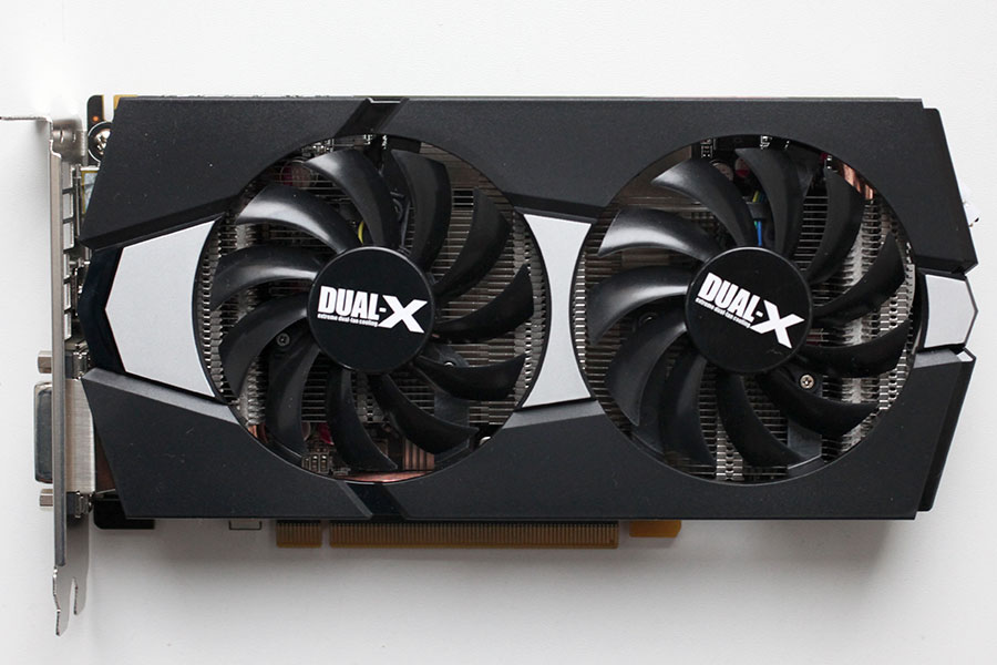

The Sapphire R7 265 looks very much like the existing Sapphire HD 7850 Dual-X. The cooler shroud also takes its inspiration from the company's R9 270. Dimensions of the card are 22 x 11.5 cm.
Installation requires two slots in your system.

Display connectivity options include two DVI ports, one DisplayPort, and one HDMI port. You may use all outputs at the same time, so triple-monitor surround gaming is possible with one card.
The GPU also includes an HDMI sound device. It is HDMI 1.4a compatible, which includes HD audio and Blu-ray 3D movies support.

One CrossFire connector lets you pair two of these cards up into a multi-GPU CrossFire configuration. The R7 265 can also CrossFire with the HD 7850.
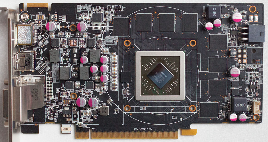

Pictured above are the front and back, showing the disassembled board. High-res versions are also available (front, back).
A Closer Look


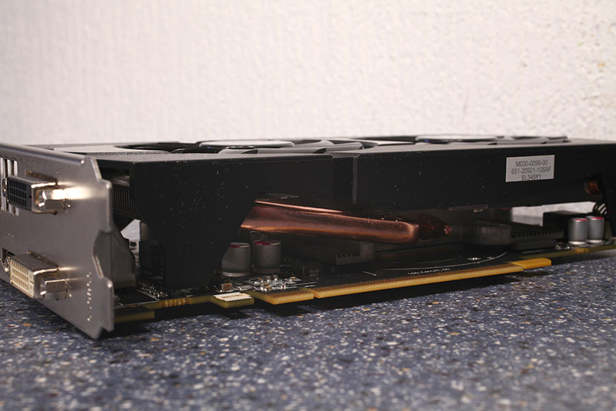
Sapphire's card uses a copper baseplate with two heatpipes to keep the card cool. The heatsink's base also cools memory chips.

The card requires one 6-pin PCI-Express power connector. This configuration is good for up to 150 W of power draw.


Our press sample came with the sticker on its antistatic bag instead of the PCB. Looks like quick re-branding to me.

Sapphire is using an OnSemi NCP4206 voltage controller on their card, which supports voltage control and monitoring via I2C.
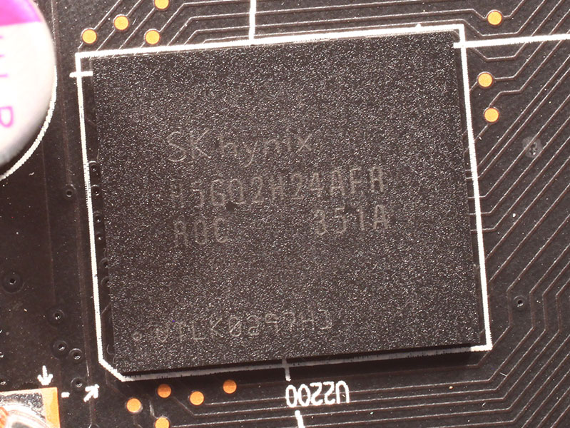
The GDDR5 memory chips are made by SK Hynix and carry the model number H5GQ2H24AFR-R0C. They are specified to run at 1500 MHz (6000 MHz GDDR5 effective).
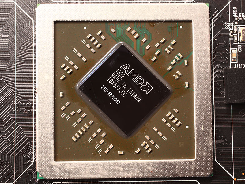
AMD's Pitcairn graphics processor uses the GCN shader architecture. It is produced on a 28 nm process at TSMC, Taiwan, and comes with 2.8 billion transistors on a 212 mm² die.
Our Patreon Silver Supporters can read articles in single-page format.
Jul 30th, 2025 04:23 CDT
change timezone
Latest GPU Drivers
New Forum Posts
- What antivirus do you use? (51)
- I stop using Windows as my main OS for like 4+ years (7)
- 3DMARK "LEGENDARY" (346)
- ASUS ROG Strix B850-I Gaming Wi-Fi (5)
- 5070ti or 9070xt? (66)
- [Intel AX1xx/AX2xx/AX4xx/AX16xx/BE2xx/BE17xx] Intel Modded Wi-Fi Driver with Intel® Killer™ Features (377)
- Windows 12 (243)
- Slow textures problems and Pop in objects on new system. RTX 5080 (31)
- TPU's Rosetta Milestones and Daily Pie Thread (2415)
- RX6800XT Gigabyte Gaming OC not giving image while being on "OC" switch and even sometimes while being on "silent" switch. (14)
Popular Reviews
- Herman Miller Logitech G Embody Review - No Pain, No Gain
- MSI Claw 8 AI+ A2VM Review
- Lenovo Legion 5i (15IRX10) Review - Feature-Rich and Wallet Friendly
- Lian Li O11 Dynamic Mini V2 Review
- Upcoming Hardware Launches 2025 (Updated May 2025)
- Noctua NF-A12x25 G2 PWM Fan Review
- Sapphire Radeon RX 9060 XT Pulse OC 16 GB Review - An Excellent Choice
- AMD Ryzen 7 9800X3D Review - The Best Gaming Processor
- AQIRYS Sirius Pro Review
- NVIDIA GeForce RTX 5050 8 GB Review
TPU on YouTube
Controversial News Posts
- AMD's Upcoming UDNA / RDNA 5 GPU Could Feature 96 CUs and 384-bit Memory Bus (134)
- AMD Radeon RX 9070 XT Gains 9% Performance at 1440p with Latest Driver, Beats RTX 5070 Ti (131)
- Intel "Nova Lake-S" Core Ultra 3, Ultra 5, Ultra 7, and Ultra 9 Core Configurations Surface (110)
- DDR6 Memory Arrives in 2027 with 8,800-17,600 MT/s Speeds (101)
- AMD Sampling Next-Gen Ryzen Desktop "Medusa Ridge," Sees Incremental IPC Upgrade, New cIOD (97)
- Intel CEO Confirms SMT To Return to Future CPUs (95)
- NVIDIA Becomes First Company Ever to Hit $4 Trillion Market-Cap (94)
- Windows 12 Delayed as Microsoft Prepares Windows 11 25H2 Update (92)