 62
62
Sapphire Radeon RX 6950 XT Nitro+ Pure Review
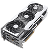
Test Setup »High-resolution PCB Pictures
These pictures are for the convenience of volt modders and people who would like to see all the finer details on the PCB. Feel free to link back to us and use these in your articles, videos or forum posts.
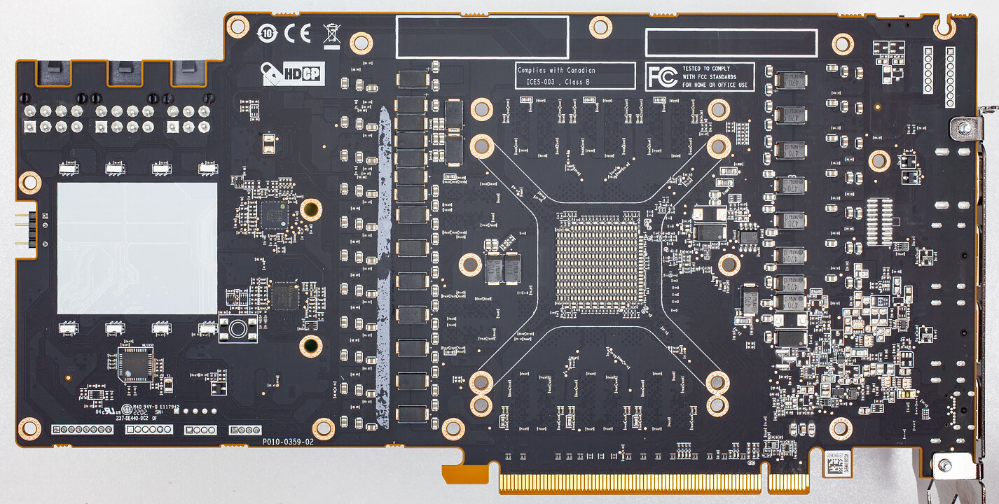
High-res versions are also available (front, back).
Circuit Board (PCB) Analysis
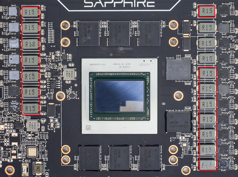

The GPU VRM is powered by the incredibly high-end Infineon XDPE132G5D running 15 power phases.

International Rectifier TDA21490 DrMOS chips are used for GPU voltage; they are rated for 90 A of current each.


Memory voltage uses a three-phase design and is generated by an IRF35217 controller.

For memory, TDA21472 DrMOS chips are used, with a 72 A rating.
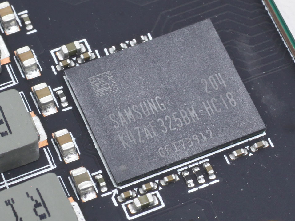
The GDDR6 memory chips are made by Samsung and carry the model number K4ZAF325BM-HC18. They are specified to run at 2250 MHz (18 Gbps GDDR6 effective).

AMD's Navi 21 graphics processor is the company's most powerful RDNA 2 chip. It is fabricated using a 7 nanometer production process at TSMC Taiwan; its transistor count is 26.8 billion, and the die size is 520 mm².
Jul 30th, 2025 02:57 CDT
change timezone
Latest GPU Drivers
New Forum Posts
- [Intel AX1xx/AX2xx/AX4xx/AX16xx/BE2xx/BE17xx] Intel Modded Wi-Fi Driver with Intel® Killer™ Features (377)
- Windows 12 (243)
- What antivirus do you use? (50)
- 5070ti or 9070xt? (65)
- I stop using Windows as my main OS for like 4+ years (6)
- TPU's Rosetta Milestones and Daily Pie Thread (2415)
- RX6800XT Gigabyte Gaming OC not giving image while being on "OC" switch and even sometimes while being on "silent" switch. (14)
- 9070XT Bios Flashed Fail (7)
- The Official Linux/Unix Desktop Screenshots Megathread (796)
- Post your 7-Zip v22.01 scores (437)
Popular Reviews
- Herman Miller Logitech G Embody Review - No Pain, No Gain
- Lenovo Legion 5i (15IRX10) Review - Feature-Rich and Wallet Friendly
- MSI Claw 8 AI+ A2VM Review
- Lian Li O11 Dynamic Mini V2 Review
- Upcoming Hardware Launches 2025 (Updated May 2025)
- Noctua NF-A12x25 G2 PWM Fan Review
- Sapphire Radeon RX 9060 XT Pulse OC 16 GB Review - An Excellent Choice
- AMD Ryzen 7 9800X3D Review - The Best Gaming Processor
- AQIRYS Sirius Pro Review
- NVIDIA GeForce RTX 5050 8 GB Review
TPU on YouTube
Controversial News Posts
- AMD's Upcoming UDNA / RDNA 5 GPU Could Feature 96 CUs and 384-bit Memory Bus (134)
- AMD Radeon RX 9070 XT Gains 9% Performance at 1440p with Latest Driver, Beats RTX 5070 Ti (131)
- Intel "Nova Lake-S" Core Ultra 3, Ultra 5, Ultra 7, and Ultra 9 Core Configurations Surface (110)
- DDR6 Memory Arrives in 2027 with 8,800-17,600 MT/s Speeds (101)
- AMD Sampling Next-Gen Ryzen Desktop "Medusa Ridge," Sees Incremental IPC Upgrade, New cIOD (97)
- Intel CEO Confirms SMT To Return to Future CPUs (95)
- NVIDIA Becomes First Company Ever to Hit $4 Trillion Market-Cap (94)
- Windows 12 Delayed as Microsoft Prepares Windows 11 25H2 Update (92)