 39
Sapphire Radeon RX 7600 Pulse OC Review
(39 Comments) »Introduction

The Sapphire Radeon RX 7600 Pulse OC is the company's close-to-reference custom design rendition of the newly launched AMD Radeon RX 7600. The Pulse series of graphics cards by Sapphire represent the value end of the company's custom-design series, and is designed for those who just want an RX 7600 graphics card that they can install and forget about. Sapphire still puts in work to make its Pulse series some of the quietest custom-designs out there. The AMD Radeon RX 7600 represents an unexpected jump by AMD from the enthusiast-segment RX 7900 series, down to the mid-range, with no performance-segment RX 7700-series or RX 7800-series launches along the way. The RX 7600 comes with all of the latest technologies the company has introduced with its latest RDNA 3 generation.

The Radeon RX 7600 is based on AMD's latest RDNA 3 graphics architecture, although the silicon itself is based on the slightly older 6 nm foundry node, not the latest 5 nm. AMD probably thinks it can pull off a mid-range GPU from this generation on the older node with minimal performance/Watt losses compared to the competition, which comes from NVIDIA's GeForce RTX 4060 series. The RDNA 3 graphics architecture debuts a completely redesigned dual-compute unit (CU), with dual issue-rate SIMD machinery that supports new math formats; the company's second-generation Ray Accelerator that offers a 50% increase in ray intersection performance over RDNA 2, and the new AI Accelerators, which speed up matrix multiplication and other forms of math relevant to AI deep-learning neural net building and training (essentially AMD's version of a Tensor core).
The RX 7600 maxes out the "Navi 33" silicon it is based on, enabling all 32 RDNA 3 compute units physically present, which work out to 2,048 stream processors, 32 Ray Accelerators, 64 AI accelerators, 128 TMUs, and 64 ROPs. Just like the shader counts, the memory sub-system is unchanged from the previous generation, albeit generationally improved. The RX 7600 enjoys 8 GB of GDDR6 memory across a 128-bit memory bus. This runs at higher 18 Gbps speeds, and the company is using second-generation Infinity Cache, a 32 MB last-level cache on the GPU that speeds up the memory sub-system. The RX 7600 also gets AMD Radiance Display Engine, which offers support for the latest DisplayPort 2.1a and HDMI 2.1 connector standards, while the RDNA 3 media engine offers dual simultaneous media encode streams.
The Sapphire RX 7600 Pulse OC features a simple aluminium fin-stack cooler with a fan profile that prioritizes low noise, and a PCB that's very close to the AMD reference design. The card is meant to be compact and highly compatible across most gaming PC case types. Power is drawn from a single 8-pin PCIe power connector. Sapphire offers a tiny factory-overclock with this card, which sees the Game clock set at 2356 MHz, compared to 2250 MHz AMD reference. The memory is untouched at 18 Gbps. Sapphire has decided to price the RX 7600 Pulse OC at the AMD MSRP of $269.
| Price | Cores | ROPs | Core Clock | Boost Clock | Memory Clock | GPU | Transistors | Memory | |
|---|---|---|---|---|---|---|---|---|---|
| RX 5500 XT | $170 | 1408 | 32 | 1717 MHz | 1845 MHz | 1750 MHz | Navi 14 | 6400M | 4 GB, GDDR6, 128-bit |
| RX 5600 XT | $190 | 2304 | 64 | 1375 MHz | 1560 MHz | 1500 MHz | Navi 10 | 10300M | 6 GB, GDDR6, 192-bit |
| RX 6500 XT | $150 | 1024 | 32 | 2685 MHz | 2825 MHz | 2248 MHz | Navi 24 | 5400M | 4 GB, GDDR6, 64-bit |
| RTX 2060 | $180 | 1920 | 48 | 1365 MHz | 1680 MHz | 1750 MHz | TU106 | 10800M | 6 GB, GDDR6, 192-bit |
| RX Vega 64 | $320 | 4096 | 64 | 1247 MHz | 1546 MHz | 953 MHz | Vega 10 | 12500M | 8 GB, HBM2, 2048-bit |
| RX 5700 XT | $180 | 2560 | 64 | 1605 MHz | 1755 MHz | 1750 MHz | Navi 10 | 10300M | 8 GB, GDDR6, 256-bit |
| RTX 3050 | $260 | 2560 | 32 | 1552 MHz | 1777 MHz | 1750 MHz | GA106 | 12000M | 8 GB, GDDR6, 128-bit |
| RTX 2070 | $230 | 2304 | 64 | 1410 MHz | 1620 MHz | 1750 MHz | TU106 | 10800M | 8 GB, GDDR6, 256-bit |
| Arc A750 | $250 | 3584 | 112 | 2050 MHz | N/A | 2000 MHz | ACM-G10 | 21700M | 8 GB, GDDR6, 256-bit |
| RX 6600 | $210 | 1792 | 64 | 2044 MHz | 2491 MHz | 1750 MHz | Navi 23 | 11060M | 8 GB, GDDR6, 128-bit |
| RX 6600 XT | $250 | 2048 | 64 | 2359 MHz | 2589 MHz | 2000 MHz | Navi 23 | 11060M | 8 GB, GDDR6, 128-bit |
| RTX 3060 | $300 | 3584 | 48 | 1320 MHz | 1777 MHz | 1875 MHz | GA106 | 12000M | 12 GB, GDDR6, 192-bit |
| RTX 4060 | $300 | 3072 | 32 | 1830 MHz | 2460 MHz | 2125 MHz | AD107 | unknown | 8 GB, GDDR6, 128-bit |
| RX 7600 | $270 | 2048 | 64 | 2250 MHz | 2625 MHz | 2250 MHz | Navi 33 | 13300M | 8 GB, GDDR6, 128-bit |
| Sapphire RX 7600 Pulse OC | $270 | 2048 | 64 | 2356 MHz | 2754 MHz | 2250 MHz | Navi 33 | 13300M | 8 GB, GDDR6, 128-bit |
| Arc A770 | $290 | 4096 | 128 | 2100 MHz | N/A | 2187 MHz | ACM-G10 | 21700M | 16 GB, GDDR6, 256-bit |
| RTX 2080 | $260 | 2944 | 64 | 1515 MHz | 1710 MHz | 1750 MHz | TU104 | 13600M | 8 GB, GDDR6, 256-bit |
| RTX 3060 Ti | $320 | 4864 | 80 | 1410 MHz | 1665 MHz | 1750 MHz | GA104 | 17400M | 8 GB, GDDR6, 256-bit |
| RTX 4060 Ti | $400 | 4352 | 48 | 2310 MHz | 2535 MHz | 2250 MHz | AD106 | 22900M | 8 GB, GDDR6, 128-bit |
| RX 6700 XT | $320 | 2560 | 64 | 2424 MHz | 2581 MHz | 2000 MHz | Navi 22 | 17200M | 12 GB, GDDR6, 192-bit |
| RTX 2080 Ti | $400 | 4352 | 88 | 1350 MHz | 1545 MHz | 1750 MHz | TU102 | 18600M | 11 GB, GDDR6, 352-bit |
| RTX 3070 | $350 | 5888 | 96 | 1500 MHz | 1725 MHz | 1750 MHz | GA104 | 17400M | 8 GB, GDDR6, 256-bit |
| RTX 3070 Ti | $420 | 6144 | 96 | 1575 MHz | 1770 MHz | 1188 MHz | GA104 | 17400M | 8 GB, GDDR6X, 256-bit |
| RX 6800 | $470 | 3840 | 96 | 1815 MHz | 2105 MHz | 2000 MHz | Navi 21 | 26800M | 16 GB, GDDR6, 256-bit |
Architecture


AMD Radeon RX 7600 is based on the Navi 33 silicon that the company chose to built on the older 6 nm (DUV) foundry node that significantly lower transistor density than the 5 nm EUV node that the Navi 31 powering the RX 7900 series is based on. The chip has a die-area of 204 mm², and transistor count of 13.3 billion (for reference, NVIDIA is able to cram 22.9 billion transistors into a 190 mm² silicon using 5 nm, with the AD106 powering the RTX 4060 Ti). The GPU has essentially the same component hierarchy as the previous-generation Navi 23. Its host interface is PCI-Express 4.0 x8, and power is drawn from a single 8-pin PCIe power connector, which is sufficient, given the gaming total board power for the RX 7600 of 169 W. The GPU features a 128-bit wide GDDR6 memory interface, and 8 GB is the standard memory size for the RX 7600.
AMD hasn't put out a block diagram of the Navi 33, but it features two Shader Engines (compared to six on the Navi 31). Each of these has 8 RDNA 3 Dual-Compute Units (16 CU), which share Raster machinery, and Render Backends. The GPU features Centralized Geometry Processors, asynchronous compute engines, and geometry processors shared among the two Shader Engines. Given its CU count of 32, we arrive at 2,048 stream processors, 32 Ray Accelerators, 64 AI Accelerators, 128 TMUs, and 64 ROPs. The GPU uses a 2nd Gen 32 MB Infinity Cache memory that cushions data access to the memory.


Much of the architectural innovation is this generation is with the RDNA 3 Dual-Compute Unit (or Compute Unit pair). The "Navi 33" GPU physically features 32 compute units spread across two Shader Engines. AMD claims that at the same engine clocks, the RDNA 3 CU offers a 17.4% IPC increase over the RDNA 2 CU.


The new RDNA 3 CU introduces multi-precision capability for the 64 stream processors per CU: operating either as 1x SIMD64 or 2x SIMD32 units. The Vector Unit that houses these SIMD units can either function as a SIMD execution mechanism, or as a Matrix execution unit, thanks to the new AI Matrix Accelerator, which provides a 2.7x matrix multiplication performance uplift versus conventional SIMD execution. Also added are support for the Bfloat16 instruction-set, and SIMD8 execution. The GPU hence enjoys AI hardware-acceleration that can be leveraged in future feature-additions relevant to gamers, such as FSR 3.0. Game developers will also look for ways to exploit accelerated AI, now that all three brands feature it (NVIDIA Tensor cores and Intel XMX cores).


AMD's first-generation Ray Accelerator, introduced with the RDNA 2 architecture, was the result of a hasty effort to catch up to NVIDIA with a DirectX 12 Ultimate GPU, where they developed a fixed-function hardware to calculate ray intersections, and offloaded a large chunk of RT processing to the generationally-doubled SIMD resources. With RDNA 3, they've refined the Ray Accelerator to achieve an 80% ray tracing performance uplift over the previous generation, when you add up the Ray Accelerator count, their higher engine clocks, and other hardware-level optimizations, such as early sub-tree culling, specialized box sorting modes, and reduced traversal iterations.


There is a 50% ray intersection capacity improvement for RDNA 3 thanks to these optimizations, and cycles-per-ray reduction. Besides these, AMD has also made several improvements to the geometry- and pixel-pipes, with the introduction of the new multi-draw indirect accelerator (MDIA), which reduces CPU API and driver-level overheads by gathering and parsing of multi-draw command data. At the hardware-level 12 primitives per clock is now supported compared to 8 per clock on RDNA 2, thanks to culling. The core-configuration overall enables 50% more rasterized performance per clock.


AMD has significantly improved the Display Engine of "Navi 33" over the previous-generation in terms of connectivity. The new Radiance Display Engine comes with native support for DisplayPort 2.1, which enables 8K output at up to 165 Hz refresh-rate, or 4K at up to 480 Hz, with a single cable. AMD has refined its FSR 2 algorithm to support 8K (i.e. render at a lower resolution with FSR-enhanced upscaling), to make it possible to enjoy the latest AAA titles at playable frame-rates on 8K displays. The RX 7600 gets two full-size DP 2.1 connectors, besides an HDMI 2.1b, and a USB-C with DP 1.2 passthrough. The "Navi 33" silicon receives full hardware-accelerated AV1 encode and decode capabilities. With this generation, AMD is also introducing SmartAccess Video, a feature that lets the AMD driver leverage the hardware encoders of the RDNA 2 iGPU of Ryzen 7000 desktop processors, for additional encoding performance.
Packaging


The Card


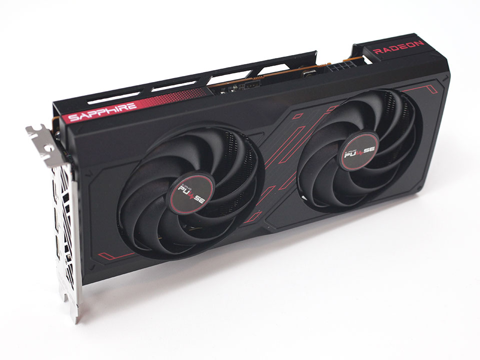
The Sapphire Radeon RX 7600 Pulse OC debuts a new cooling solution design that retains the minimalist red-on-black color scheme of the series. There's no fancy RGB lighting to be had, whatever visual uplift is from the design itself. The cooler shroud is made of plastic, but the backplate is metal.


Dimensions of the card are 24.0 x 12.0 cm, and it weighs 627 g.


Installation requires two slots in your system.
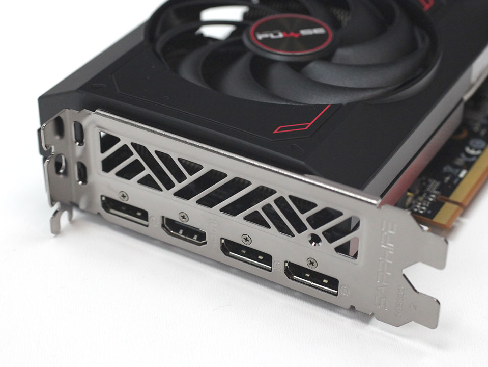
Display connectivity includes three standard DisplayPort 2.1 ports (RDNA 2 had 1.4a) and one HDMI 2.1a.
AMD has upgraded their encode/decode setup. It now comes with support for VP9, H.264, H.265 and AV1 decode, and encoding is supported for H.264, H.265 and AV1.

The card's sole power connector is an 8-pin PCIe. Together with 75 W PCIe slot power, this configuration is rated for 225 W.
Teardown


Sapphire Radeon RX 7600 Pulse OC exudes simplicity, so taking it apart is pretty straightforward. The cooler shroud comes off more easily than the rest of the heatsink, so you can clean its fans without having to take the whole cooler apart (and disturb the TIM or thermal pads).


The main heatsink uses a single aluminium fin-stack with its fins arranged longitudinally. A copper base-plate makes contact with the GPU and memory, there are additional contact points for the VRM.
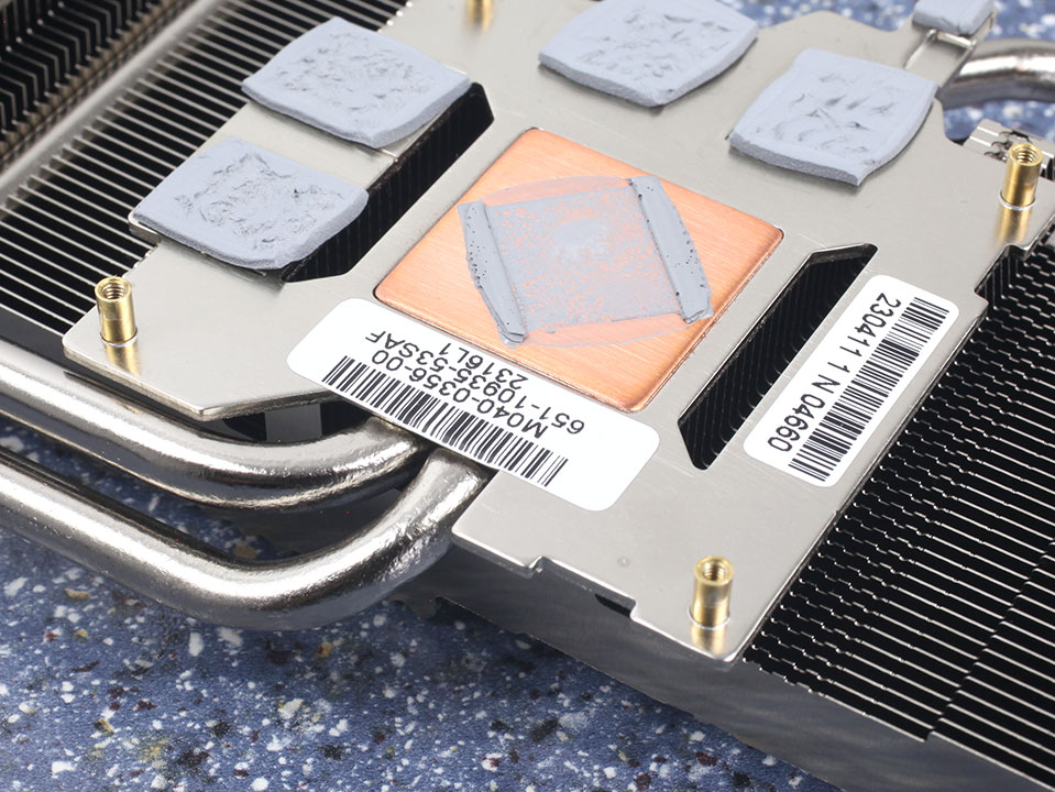
The cooler uses two heatpipes that convey heat through the fin-stack in an S-shape.


The backplate is made of metal, and its three-dimensional design counteracts PCB sagging over time.
High-resolution PCB Pictures
These pictures are for the convenience of volt modders and people who would like to see all the finer details on the PCB. Feel free to link back to us and use these in your articles, videos or forum posts.

High-resolution versions are also available (front, back).
Our Patreon Silver Supporters can read articles in single-page format.
Nov 14th, 2026 12:18 CST
change timezone
Latest GPU Drivers
New Forum Posts
- Tell me about your favourite graphics card (57)
- no "PhysX" workable (10)
- TPU's Nostalgic Hardware Club (22162)
- What can the FX 8320 do today? Here is the answer. (30)
- Slow SSD read speeds - help! (7)
- What card do I get for VR? (29)
- Ddr4 instead of ddr5 for 9060xt 8 gb over 5060 8 gb (7)
- Your PC ATM (36414)
- Microsoft Exchange/365 outages? (62)
- Opinion on Monitor Replacement (7)
Popular Reviews
- AMD Zen 6 Technical Deep Dive
- ASUS ROG Strix B850-I Gaming Wi-Fi7 W Review
- Corsair HX1000i Shift Crystal Review
- NZXT C1200 Platinum Review
- Upcoming Hardware Launches 2027 (Updated Nov 2026)
- Montech King 95 3D PRO Review
- NZXT H7 RGB+ Review
- NZXT H5 Review
- Phantom Blade Zero Performance Benchmark Review - 35 GPUs Tested
- XPG NIMBUS PLUS Review - Mid-range Chair With Strong Competitors
TPU on YouTube
Controversial News Posts
- NVIDIA Co-Founder and CEO Jensen Huang Officially Resigns (399)
- OpenAI CEO Argues Home PCs Waste the World's Limited DRAM Supply (152)
- NVIDIA Launches Investigation Into Jensen Huang's Relationship With Suspected Chinese Spy (136)
- Intel "Raptor Lake Next" 16-Core and 20-Core CPUs Surface (130)
- Legendary Game Studio BioWare Shuts Down Following EA Layoffs (104)
- Dell CEO Says the Memory Shortage Will Get Worse in 2027 (95)
- NVIDIA GeForce RTX 50-Series Scheduled for up to $500 Price Hike This Week (89)
- Modder Fits RTX 5090 With Four 8-Pin Connectors, Halving Current per Wire (80)