 553
553
AMD Radeon VII 16 GB Review
Circuit Board Analysis »The Card

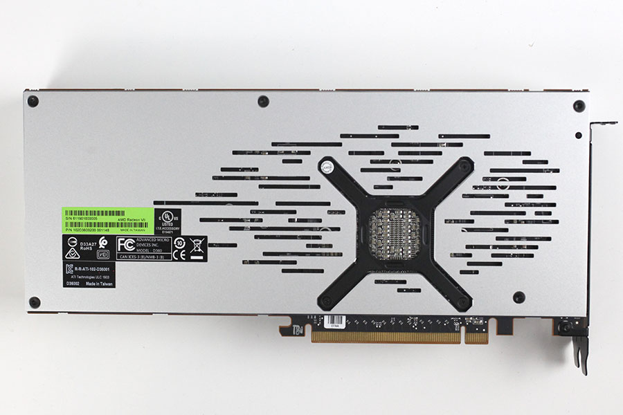
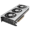
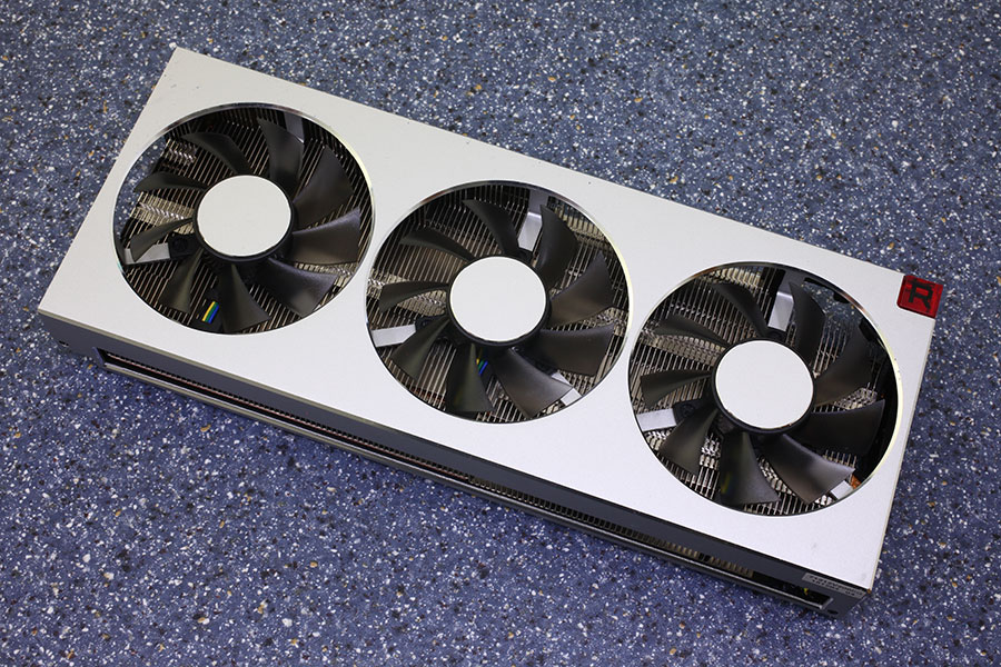
The Radeon VII comes in an aluminium-clad design that's dominated by brushed metal surfaces, which give the card a high-quality premium look and feel. This is the first time an AMD reference design comes with three fans to maximize airflow. The metal backplate matches the visual theme of the main cooler. Dimensions of the card are 27.0 x 12.0 cm, which ensures it will fit nearly all cases except for the most compact ones.

Installation requires two slots in your system.
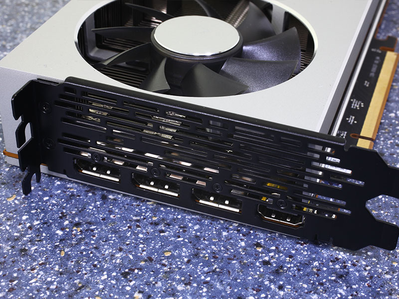
Display connectivity options include three standard DisplayPort 1.4a and one HDMI 2.0b port. This is the same output configuration as on Vega 56 and Vega 64.
The HDMI port is version 2.0, and DisplayPort uses 1.4 HBR3, MST, and HDR. This enables support for 4K @ 120 Hz, 5K @ 60 Hz, or 8K @ 60 Hz. Supported HDR configurations are 4K60, 4K120, and 5K60, just like first-generation Vega. GPU-accelerated encoding is capable of HEVC/H.264 at up to 1080p240, 1440p120, and 2160p60. Hardware-based decoding works at up to 4K60 for H.264, H.265, and VP9 (shader-assisted).

The board uses two 8-pin power connectors. This input configuration is specified for up to 375 watts of power draw.

AMD CrossFire has been running over the PCI-Express bus for a few generations now. The Vega Series is no different.
Disassembly

Once the backplate is removed, the main cooling assembly comes off easily. The whole disassembly process is fairly straightforward and much easier than on the NVIDIA RTX 2070 or RTX 2060.
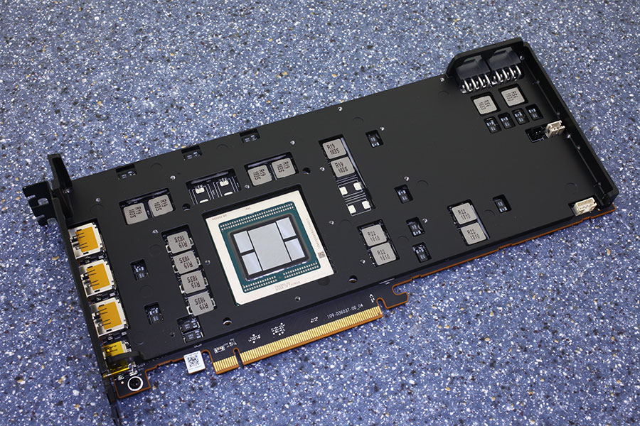


Only after finishing the full disassembly did I notice that there are actually two pieces that make up the main cooler: a black metal baseplate that cools voltage regulation circuitry and the main heatsink with the copper baseplate, heatpipes, and three fans attached to it.

Note the black thermal pad AMD is using. It's of a fairly solid substance that's sticky and really difficult to get off unless you dissolve it (I used ArctiClean). It's also interesting how the thermal pad broke when the cooler came off—it is definitely not reusable. It looks like it got more sticky at the hottest spot (in the center of the GPU die), so the outer areas stuck with the cooler while the center part stuck to the GPU chip. After a bit of research, it looks like the pad is a Hitachi TC-HM03 and uses a mix of graphite strands (pure carbon) and epoxy to create a thick, reusable, high conductivity thermal pad. I'm not 100% sure why AMD went with this instead of traditional thermal paste. The GPU surface, including the HBM chips, seems perfectly flat, unlike some earlier Vega 10 cards where height differences had to be filled out by thermal paste.
In the overclocking section of this review, we'll also describe how we significantly improved thermal performance by using regular paste with increased mounting pressure.
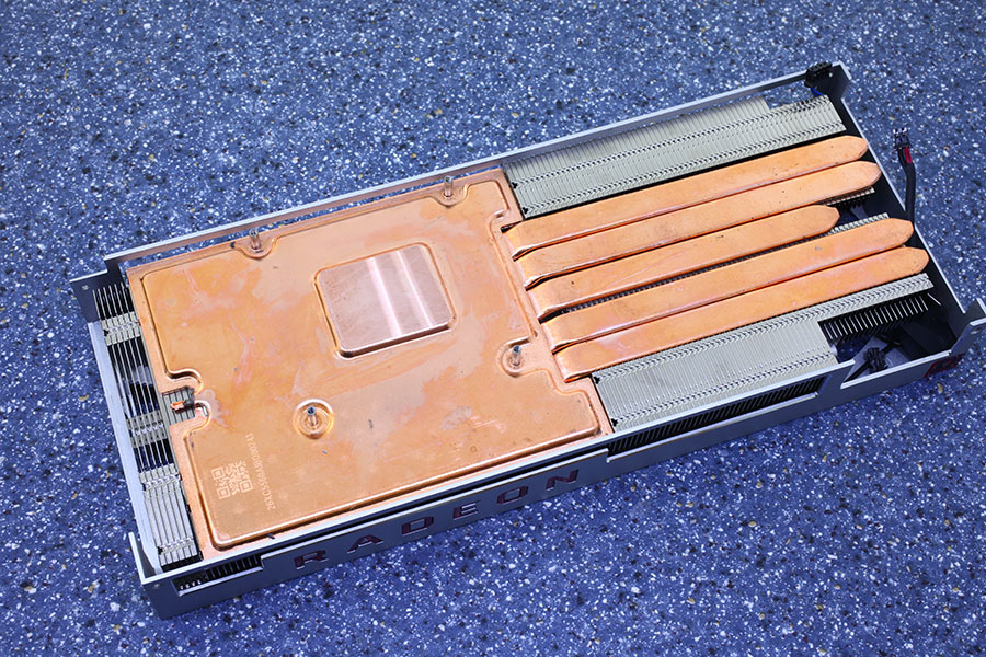
Once cleaned up, you can see the large copper vapor-chamber that soaks up heat from the GPU surface and the five heatpipes attached to it. These heatpipes spread heat to the edges of the fin-stack.


The backplate is made out of metal and protects the card against damage during installation and handling.
On the next page, we dive deep into the PCB layout and VRM configuration.
Apr 26th, 2024 13:43 EDT
change timezone
Latest GPU Drivers
New Forum Posts
- DTS:X APO4 + DTS Interactive for Most Devices [USB Supported] (305)
- The Official Linux/Unix Desktop Screenshots Megathread (702)
- What's your latest tech purchase? (20352)
- hacked (73)
- im new to throttelstop and i think i messed it up by copying others any hints would be very much aprreciated (5)
- 2022-X58/1366 PIN Motherboards NVME M.2 SSD BIOS MOD Collection (657)
- DTS DCH Driver for Realtek HDA [DTS:X APO4 + DTS Interactive] (1909)
- checkup (1)
- Help me to OC my 5700X (10)
- XFX RX470 8GB no video and error 43 (28)
Popular Reviews
- HYTE THICC Q60 240 mm AIO Review
- MOONDROP x Crinacle DUSK In-Ear Monitors Review - The Last 5%
- Alienware Pro Wireless Gaming Keyboard Review
- Upcoming Hardware Launches 2023 (Updated Feb 2024)
- Logitech G Pro X Superlight 2 Review - Updated with 4000 Hz Tested
- Thermalright Phantom Spirit 120 EVO Review
- AMD Ryzen 5 7600 Review - Affordable Zen 4 for the Masses
- FiiO K19 Desktop DAC/Headphone Amplifier Review
- ASUS Radeon RX 7900 GRE TUF OC Review
- RTX 4090 & 53 Games: Ryzen 7 5800X vs Ryzen 7 5800X3D Review
Controversial News Posts
- Windows 11 Now Officially Adware as Microsoft Embeds Ads in the Start Menu (128)
- Sony PlayStation 5 Pro Specifications Confirmed, Console Arrives Before Holidays (117)
- NVIDIA Points Intel Raptor Lake CPU Users to Get Help from Intel Amid System Instability Issues (106)
- AMD "Strix Halo" Zen 5 Mobile Processor Pictured: Chiplet-based, Uses 256-bit LPDDR5X (102)
- US Government Wants Nuclear Plants to Offload AI Data Center Expansion (98)
- AMD's RDNA 4 GPUs Could Stick with 18 Gbps GDDR6 Memory (92)
- Developers of Outpost Infinity Siege Recommend Underclocking i9-13900K and i9-14900K for Stability on Machines with RTX 4090 (85)
- Windows 10 Security Updates to Cost $61 After 2025, $427 by 2028 (84)