 51
51
ASUS GeForce GTX 980 Ti Matrix 6 GB Review
Test Setup »A Closer Look
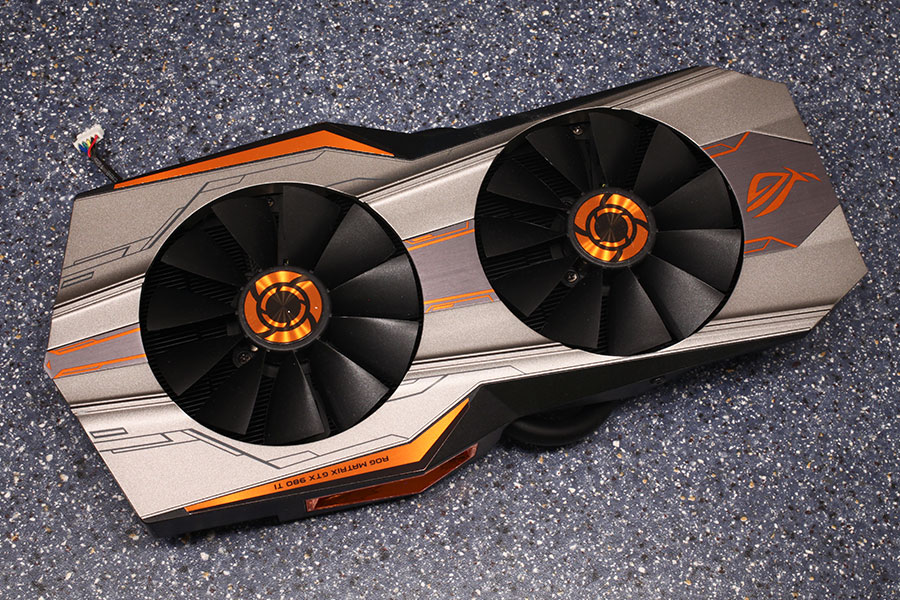

With its all-black design, ASUS' heatsink looks ultra-stylisch. Five heatpipes which make direct contact with the GPU's surface can be found on the base.

Taking a look at the card without its primary heatsink attached, you can see a secondary heatsink that cools the voltage regulation circuitry. Near the top-edge is a metal bar that is there as reinforcement to make sure the card doesn't sag once it has been installed into a case.

Power delivery requires two 8-pin PCI-Express power connectors. This configuration is specified for up to 375 W power draw.

Near the SLI connector is a switch that toggles between the normal and LN2 BIOS. This switch is only enabled after bridging the "Enable LN2" solder points.


ASUS has included a bunch of enthusiast overclocking options on their Matrix. Here's a list from left to right:
- Molex power connector for the memory defroster (not needed for normal operation). When using liquid nitrogen, the back of the card will freeze with ice due to condensation, which can short circuits and result in cold bugs. The memory heater is activated by connecting a solder bridge and wiring a button to the corresponding XJ16 pins.
- You will find a bunch of unlabeled solder vias near XJ16. These are used to connect the VGA Hotwire feature on a supporting motherboard, but you could also emulate that behavior with trimpots and a DMM.
- The big "safe mode" button will restore the default clocks and voltages if you saved them to the VBIOS using ASUS GPUTweak.
- On the other side of that button is the "enable LN2" solder pad, which needs to be connected to enable the BIOS switch for you to run the second BIOS that is optimized for liquid-nitrogen usage.
- There are six solder vias all the way to the right and near the power connectors of which I'm not sure what they do (I've asked ASUS).

ASUS is using their own voltage controller, which seems to be a rebranded CHiL 8318.

The GDDR5 memory chips are made by Hynix and carry the model number H5GQ4H24MFR-R2C. They are specified to run at 1750 MHz (7000 MHz GDDR5 effective).

NVIDIA's GM200 graphics processor is the company's flagship GPU. It is produced on a 28 nm process at TSMC, Taiwan, with a transistor count of 8.0 billion and a die size of 601 mm².
May 7th, 2024 09:44 EDT
change timezone
Latest GPU Drivers
New Forum Posts
- How to check flatness of CPUs and coolers - INK and OPTICAL INTERFERENCE methods (118)
- Would you guys be ok with 70C idle temp on NVME storage. (28)
- Is this Sapphire PULSE RX 5600 XT legit or fake? (43)
- Arctic MX-6 shelf life is just a couple months? (94)
- not impressed - nvme vs ssd (27)
- 6800XT Red Devil with 18°C difference from Core to Hotspot (5)
- Keysfan (22)
- Ghetto Mods (4335)
- The Official Thermal Interface Material thread (1172)
- Dota 2 GPU performance test (5)
Popular Reviews
- Finalmouse UltralightX Review
- Corsair iCUE Link RX120 RGB 120 mm Fan Review
- Cougar Hotrod Royal Gaming Chair Review
- Meze Audio LIRIC 2nd Generation Closed-Back Headphones Review
- Upcoming Hardware Launches 2023 (Updated Feb 2024)
- ASRock NUC BOX-155H (Intel Core Ultra 7 155H) Review
- AMD Ryzen 7 7800X3D Review - The Best Gaming CPU
- ASUS Radeon RX 7900 GRE TUF OC Review
- Montech Sky Two GX Review
- HYTE THICC Q60 240 mm AIO Review
Controversial News Posts
- Intel Statement on Stability Issues: "Motherboard Makers to Blame" (250)
- AMD to Redesign Ray Tracing Hardware on RDNA 4 (191)
- Windows 11 Now Officially Adware as Microsoft Embeds Ads in the Start Menu (167)
- NVIDIA to Only Launch the Flagship GeForce RTX 5090 in 2024, Rest of the Series in 2025 (124)
- Sony PlayStation 5 Pro Specifications Confirmed, Console Arrives Before Holidays (119)
- AMD's RDNA 4 GPUs Could Stick with 18 Gbps GDDR6 Memory (114)
- NVIDIA Points Intel Raptor Lake CPU Users to Get Help from Intel Amid System Instability Issues (106)
- AMD Ryzen 9 7900X3D Now at a Mouth-watering $329 (104)