Report an Error
Western Digital RED SN700 1 TB
1 TB
Capacity
WD 20-82-00700
Controller
TLC
Flash
PCIe 3.0 x4
Interface
M.2 2280
Form Factor


Hexus
PCB Front

Hexus
DRAM
Hexus
Flash

Controller

NAND Die
The Western Digital RED SN700 is a solid-state drive in the M.2 2280 form factor, launched on September 28th, 2021. It is available in capacities ranging from 250 GB to 4 TB. This page reports specifications for the 1 TB variant. With the rest of the system, the Western Digital RED SN700 interfaces using a PCI-Express 3.0 x4 connection. The SSD controller is the 20-82-00700-A2 Triton MP28 from WD, a DRAM cache chip is available. Western Digital has installed 96-layer TLC NAND flash on the RED SN700, the flash chips are made by Toshiba. To improve write speeds, a pseudo-SLC cache is used, so bursts of incoming writes are processed more quickly. The RED SN700 is rated for sequential read speeds of up to 3,430 MB/s and 3,000 MB/s write; random IOPS reach up to 515K for reads and 560K for writes.
At its launch, the SSD was priced at 145 USD. The warranty length is set to five years, which is an excellent warranty period. Western Digital guarantees an endurance rating of 2000 TBW, a high value.
At its launch, the SSD was priced at 145 USD. The warranty length is set to five years, which is an excellent warranty period. Western Digital guarantees an endurance rating of 2000 TBW, a high value.
Solid-State-Drive
| Capacity: | 1 TB (1000 GB) |
|---|---|
| Variants: | 250 GB 500 GB 1 TB 2 TB 4 TB |
| Overprovisioning: | 92.7 GB / 10.0 % |
| Production: | Active |
| Released: | Sep 28th, 2021 |
| Price at Launch: | 145 USD |
| Part Number: | WDS100T1R0C |
| Market: | Consumer |
Physical
| Form Factor: | M.2 2280 |
|---|---|
| Interface: | PCIe 3.0 x4 |
| Protocol: | NVMe 1.3 |
| Power Draw: |
0.10 W (Idle) Unknown (Avg) Unknown (Max) |
Controller
| Manufacturer: | WD |
|---|---|
| Name: | 20-82-00700-A2 Triton MP28 |
| Architecture: | ARM 32-bit Cortex-R |
| Core Count: | Triple-Core |
| Foundry: | TSMC |
| Process: | 28 nm |
| Flash Channels: | 8 @ 800 MT/s |
| Chip Enables: | 4 |
| Controller Features: | DRAM (enabled) |
NAND Flash
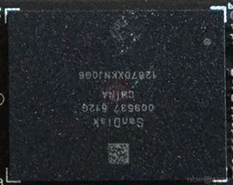
| Manufacturer: | Toshiba |
|---|---|
| Name: | BiCS4 |
| Rebranded: | 009537 512G (Rebranded by SanDisk) |
| Type: | TLC |
| Technology: | 96-layer |
| Speed: | 800 MT/s |
| Capacity: | 2 chips @ 4 Tbit |
| ONFI: | 4.0 |
| Toggle: | 3.0 |
| Topology: | Charge Trap |
| Process: | 19 nm |
| Die Size: | 86 mm² (6.0 Gbit/mm²) |
| Dies per Chip: | 8 dies @ 512 Gbit |
| Planes per Die: | 2 |
| Decks per Die: | 2 |
| Word Lines: |
109 per NAND String
88.1% Vertical Efficiency |
| Read Time (tR): | 58 µs |
| Program Time (tProg): | 561 µs |
| Die Read Speed: | 551 MB/s |
| Die Write Speed: | 57 MB/s |
| Endurance: (up to) |
3000 P/E Cycles
(30000 in SLC Mode) |
| Page Size: | 16 KB |
| Block Size: | 1152 Pages |
| Plane Size: | 1822 Blocks |
DRAM Cache
| Type: | DDR4-2666 CL18 |
|---|---|
| Name: | Micron MT40A512M16LY-075:E (D9WFH) |
| Capacity: |
1024 MB
(1x 1024 MB) |
| Organization: | 8Gx16 |
Performance
| Sequential Read: | 3,430 MB/s |
|---|---|
| Sequential Write: | 3,000 MB/s |
| Random Read: | 515,000 IOPS |
| Random Write: | 560,000 IOPS |
| Endurance: | 2000 TBW |
| Warranty: | 5 Years |
| MTBF: | 1.8 Million Hours |
| Drive Writes Per Day (DWPD): | 1.1 |
| SLC Write Cache: | Yes |
Features
| TRIM: | Yes |
|---|---|
| SMART: | Yes |
| Power Loss Protection: | No |
| Encryption: |
|
| RGB Lighting: | No |
| PS5 Compatible: | No |
Reviews
Notes
NAND Die:Read latency tR: 58 µs (ABL) |
May 2nd, 2024 02:17 EDT
change timezone
Latest GPU Drivers
New Forum Posts
- What's your latest tech purchase? (20405)
- Are all software/scheduling issues with e-cores fixed on Intel 12th to 14th Gen - Willing to give hybrid ach a chance now (80)
- 14900k - Tuned for efficiency - Gaming power draw (347)
- TPU's Nostalgic Hardware Club (18486)
- Current Sales, Bundles, Giveaways (10221)
- Throttlestop stopped working (VBS is disabled) (3)
- 7800XT Issue , amdflash bios (9)
- Arctic MX-6 shelf life is just a couple months? (72)
- AMD RX 7000 series GPU Owners' Club (1092)
- Your PC ATM (34536)
Popular Reviews
- Ugreen NASync DXP4800 Plus Review
- HYTE THICC Q60 240 mm AIO Review
- Montech Sky Two GX Review
- Upcoming Hardware Launches 2023 (Updated Feb 2024)
- MOONDROP x Crinacle DUSK In-Ear Monitors Review - The Last 5%
- Team Group T-Force Vulcan ECO DDR5-6000 32 GB CL38 Review
- AMD Ryzen 7 7800X3D Review - The Best Gaming CPU
- ASRock NUC BOX-155H (Intel Core Ultra 7 155H) Review
- Thermalright Phantom Spirit 120 EVO Review
- ASUS Radeon RX 7900 GRE TUF OC Review
Controversial News Posts
- Intel Statement on Stability Issues: "Motherboard Makers to Blame" (219)
- Windows 11 Now Officially Adware as Microsoft Embeds Ads in the Start Menu (159)
- Sony PlayStation 5 Pro Specifications Confirmed, Console Arrives Before Holidays (117)
- AMD's RDNA 4 GPUs Could Stick with 18 Gbps GDDR6 Memory (109)
- NVIDIA Points Intel Raptor Lake CPU Users to Get Help from Intel Amid System Instability Issues (106)
- AMD "Strix Halo" Zen 5 Mobile Processor Pictured: Chiplet-based, Uses 256-bit LPDDR5X (103)
- TechPowerUp Hiring: Reviewers Wanted for Motherboards, Laptops, Gaming Handhelds and Prebuilt Desktops (93)
- AMD Ryzen 9 7900X3D Now at a Mouth-watering $329 (93)