Thursday, October 1st 2009

NVIDIA 'Fermi', Tesla Board Pictured in Greater Detail, Non-Functional Dummy Unveiled
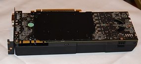
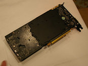
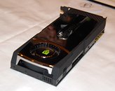
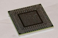
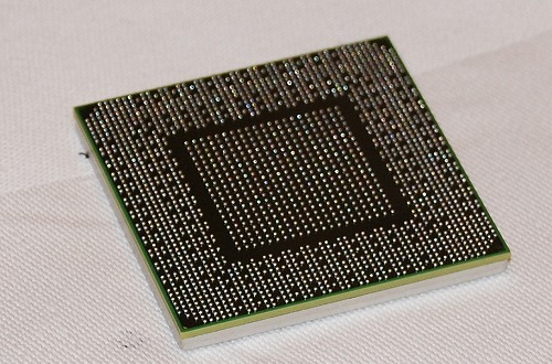
Unveiled at the footnote of the GPU Technology Conference 2009, by none other than NVIDIA CEO Jen-Hsun Huang, NVIDIA's Fermi architecture looks promising, at least in the field of GPGPU, which was extensively discussed upon in his address. The first reference board based on NVIDIA's newest 'GT300' GPU is a Tesla HPC processor card, which quickly became the face of the Fermi architecture. Singapore HardwareZone, and PCPop caught some of the first closeup pictures of the Tesla accelerator, and the GPU's BGA itself. Decked in a dash of chrome, the Tesla HPC processor card isn't particularly long, instead a great deal of compacting by its designers is evident. It draws power from one 8-pin, and 6-pin PCI-E power connectors, which aren't located next to each other. The cooler's blower also draws air from openings in the PCB, and a backplate further cools the GPU (and possibly other components located) from behind. From the looks of it, the GPU package itself isn't larger than that of the GT200 or its predecessor, the G80. Looks like NVIDIA is ready with a working prototype against all odds, after all, doesn't it? Not quite. On close inspection of the PCB, it doesn't look like a working sample. Components that are expected to have pins protruding soldered on the other side, don't have them, and the PCB seems to be abruptly ending. Perhaps it's only a dummy made to display at GTC, and give an indication of how the card ends up looking like. In other words, it doesn't look like NVIDIA has a working prototype/sample of the card they intended to have displayed the other day.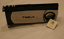
Sources:
Singapore HardwareZone, PCPop


94 Comments on NVIDIA 'Fermi', Tesla Board Pictured in Greater Detail, Non-Functional Dummy Unveiled
maybe they redesigned everything i don know
Edit: @15th Warlock: according to the site and a pic thats posted there "NVIDIA CEO and Co-Founder, Jen-Hsun Hunag proudly showing off the new GT300 based graphics card whose architecture is codenamed Fermi and will be the base for all new GeForce, Quadro and Tesla class products coming in the near future." its going to be the base of all the new card
Think of it as one of those dummies you find at mobile phone stores, of unreleased phones, etc.
@zubasa: considering they have a december relase window, they better make miracles for this to happen if all the rumors are true. For me i just need some bench and price and im sold.
Clearly this isn't a working product, the SLI connector is blocked by the backplate, and the PCI-E power connectors don't line up with the spot on the actual board.
And I pray to God that they don't actually put the PCI-E Power connectors in those locations. It is stupid to have an 8-pin on the back, and another 6-pin on the side like that. Put them both on the same side! That is the most retarded thing I've ever seen...Or at least they don't have a working sample that looks good enough to show. I'm willing to bet they have at least a few working samples, but I bet they look like ass. Refining the looks is one of the last steps in the processes, and we are a while away from seeing a finished product hit the market.
I'm really looking forward to what Nvidia has to offer in this generation. I do agree that this is a pathetic PR attempt to make nvidia FANBOYS drool over something that doesn't have any official specs to speak about.
---------
I like the shiny look of the cooler :), they should put the shiny part on top of the card so that it reflects off your sweet hardware.;)
But card is clearly fake and just for show.
:shadedshuAdd picture 1 with picture 3 = 2 connectors!
Too much of an expensive card, and Ati holding the market with DX11 and the fastest DX11 Single GPU. Not to mention that producing a GPU with over 3 billion transistors is expensive.
Onderon, learn to spam like them before calling them fanboys. :laugh:
And with the exception of bta, I have the largest postcount in this thread, and I've been here the longest, if that really matters to you, and I'll tell you IRA's post was very fanboyish and very trollish. But I'm sure he meant it more in a joking manner than a trollish/fanboyish manner.
And of course it is a PR stunt, that is exactly what these types of things are, ATi had bunches of them before the RV870 release, it is how the game works.
And there are offical specs, they came out yesterday.