Thursday, September 17th 2015

NVIDIA "Pascal" GPUs to be Built on 16 nm TSMC FinFET Node

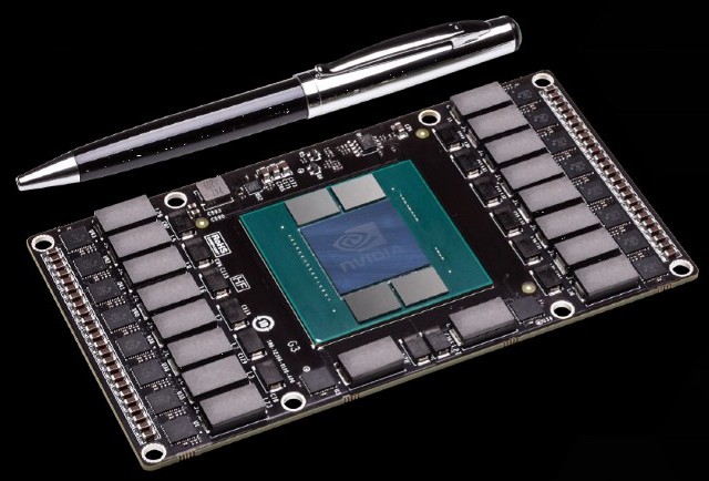
NVIDIA's next-generation GPUs, based on the company's "Pascal" architecture, will be reportedly built on the 16 nanometer FinFET node at TSMC, and not the previously reported 14 nm FinFET node at Samsung. Talks of foundry partnership between NVIDIA and Samsung didn't succeed, and the GPU maker decided to revert to TSMC. The "Pascal" family of GPUs will see NVIDIA adopt HBM2 (high-bandwidth memory 2), with stacked DRAM chips sitting alongside the GPU die, on a multi-chip module, similar to AMD's pioneering "Fiji" GPU. Rival AMD, on the other hand, could build its next-generation GCNxt GPUs on 14 nm FinFET process being refined by GlobalFoundries.
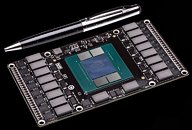
Source: BusinessKorea
Add your own comment

52 Comments on NVIDIA "Pascal" GPUs to be Built on 16 nm TSMC FinFET Node

#26
nemesis.ie
erixxDid AMD not patent this type of chip+RAM? Why not?
They believe in an open market and likely their hardware manufacturing partners would not like their market limited either.
Posted on Reply
#27
bug
PowerPCWhat tells you they won't just make the dies smaller like Intel?
They can (and probably will) use part of the savings towards a smaller die, because smaller dies are cheaper. I'll take a cheaper card that has the same performance as the GTX 970, for example.
Posted on Reply
#28
Blue-Knight

Finally, a graphics card that does not cooling or anything. I just wonder how I would connect that to my PC. :confused:
Posted on Reply
#29
bug
erixxDid AMD not patent this type of chip+RAM? Why not?
Because they did not invent HBM. Hynix did, AMD was just their first partner. Since this type of memory does not work unless someone puts it on their CPU (or whatever) die, charging for the technology would probably just slow its adoption. And that's not good when the competition (Micron) has something similar in the works (HMC). Tbh, I imagine Hynix has patented the actual implementation, they're just making it easy for others to use their memory chips.
Posted on Reply
#30
bug
Blue-KnightFinally, a graphics card that does not cooling or anything. I just wonder how I would connect that to my PC. :confused:
That's not an actual graphics card. it's a mock-up. If anything, we can learn from Fiji that these designs almost need water cooling, since now both the GPU and the memory exhaust heat through a single hotspot.
Posted on Reply
#31
ShurikN
bugIf anything, we can learn from Fiji that these designs almost need water cooling, since now both the GPU and the memory exhaust heat through a single hotspot.
Lower fab processes will most likely bring lower power, so maybe WC will not be required?
Posted on Reply
#32
Casecutter
Just love'n the idea that TSMC has to work for the business! :clap:

I'm still on the fence as to GloFo making AMD GPU's, but if they do I think we have a wield time ahead. This will mean less of the "me-too" that has been the GPU business for many years. I think perhaps this will shake-up of a lot of things; release dates, what markets are attacked first, and with what memory type. All the forum chatter will be a spinning torrent..:ohwell:.

Is TSMC holding the line on price (not like they did on the 28nm), when one (or their) biggest customer had talk of going elsewhere (Samsung), while perhaps another good customer already moved new business out? Can TSMC (shareholders) seeing lower starts stomach under-cutting the scrappy GloFo, who probably able to work aggressive margins just to get traction as anything they provide is a boom to the stock?

Could AMD move first in the $170-450 price point, with say two different chips that are (XT/Pro) so 4 variants. The lower part will hold to GDDR5 the higher part will be HBM2. But all the hinges what foundry and how soon production starts. That's the segment today where AMD is clawing back market share, and using products that have re-bands. If they stay in the control the channel, and hit with a XT mainstream card that gets up into the 980Ti they they'd ride a nice boon. That means they can let Fiji go EoL which I think is a drain on them now, and come back with a replacement Top part after couple of months.
Posted on Reply
#33
bug
ShurikNLower fab processes will most likely bring lower power, so maybe WC will not be required?
Just don't count on lower fab processes for the next few years. TSMC already dropped the ball on 22nm and intel has announced a third 14nm lineup. Clearly scaling is running into serious issues. And not unexpectedly, considering that according to some the physical limitation of silicon is around 5nm.
Posted on Reply
#34
GhostRyder
bugThat's not an actual graphics card. it's a mock-up. If anything, we can learn from Fiji that these designs almost need water cooling, since now both the GPU and the memory exhaust heat through a single hotspot.
Not really, think about the Fury Nano and the Fury regular who both use fan cooling solutions just fine. The Memory itself does not produce much heat at least compared to GDDR5.
Blue-Knight
Finally, a graphics card that does not cooling or anything. I just wonder how I would connect that to my PC. :confused:
Its not real, its a fake to show off what they are working on.

Meh, it just comes down to how they use it in the end.
Posted on Reply
#35
ShurikN
bugJust don't count on lower fab processes for the next few years. TSMC already dropped the ball on 22nm and intel has announced a third 14nm lineup. Clearly scaling is running into serious issues. And not unexpectedly, considering that according to some the physical limitation of silicon is around 5nm.
I was talking about moving from 28 to 14/16
Posted on Reply
#36
TheinsanegamerN
bugThat's not an actual graphics card. it's a mock-up. If anything, we can learn from Fiji that these designs almost need water cooling, since now both the GPU and the memory exhaust heat through a single hotspot.
Fiji was a top end uber-card. with a 350+ watt TDP, it was either water cooling or a massive air cooler. A lower end card IE fury or nano, can do just fine with air cooling. (and just look at the size of those fury coolers. fury x would need a bigger one.)

IMO, the watercooling idea should be standard on these 650+ cards. the titan x would have been even better with a water or hybrid cooler.
Posted on Reply
#37
lilhasselhoffer
OK, let's figure out lithography. Lithographic measures are actually half pitch, and not transistor size. This means that identical features on a transistor are actually 32nm away with a 16nm process. Likewise, the 28nm process currently in use would be 56nm between similar transistor features. This means that 32/56 is the actual shrink, which is 57%. This, combined with inefficiencies, lines up with the 40% quoted decrease in size for the transistors.


As far as HBM, it was a joint venture between Hynix and AMD. The intention is to use less power than DDR4, which is less than the power hungry GDDR5. They also effectively increase bandwidth, removing memory access as a block on performance: electroiq.com/blog/2013/12/amd-and-hynix-announce-joint-development-of-hbm-memory-stacks/

AMD provided research and production assistance with the product, along with demonstration of the technology. The trade was sole access to HBM1 (realistically this was supposed to make Nano/Fury), and early/prime access to HBM2. It's a huge leap forward on power consumption (GDDR5 is functionally power hungry DDR3), and it provides direct access memory. Both of these, theoretically, mean HBM should make high VRAM using applications run much better.


The "news" part of this story is those extra 2nm. AMD having those 2nm doesn't sound like a lot, but it means a 50% reduction in size rather than a 40%. That extra 10%, along with AMD ironing out the HBM issues with Fury and Nano, could spell a significant real world advantage with Arctic Islands. Be real here people, this is the closest to bashing Nvidia some people have ever come.


Edit:
Water cooling shouldn't be needed on a GPU. It should be an option, but not necessary. The point of HBM and die shrinking is exactly that. More transistors, but less voltage, means less overall heat. While I love AMD's offerings, the most recent batch of heaters they've put out are excessive. I want overclocking headroom, not a card that is already pushing thermal limits when I get it.
Posted on Reply
#38
happita
I don't know if anything is solidly confirmed by either AMD or Nvidia on which process nodes they will be producing their next generation of cards will be at. Might be wrong or haven't been keeping up with news too much lately. I wouldn't have thought that 16nm and 14nm would be a significant distance apart when comparing the advantages of only 2nm. But then again shrinking always yields some advantages be it the higher potential for a chip to perform at slightly higher clocks or to run a little cooler. We'll just have to wait and see.
Posted on Reply
#39
HumanSmoke
john_if I am not mistaken, only Intel can come out and say "I have a 14nm process". Samsung's and TSMC's 14nm and 16nm are more or less something between 20nm and 14nm or 16nm with a good dose of marketing.
Sounds like you're buying into Intel's marketing spiel from IDF14 - the one where they dumped on TSMC's and Samsung's process nodes claiming a lack of performance scaling among other things. Most of Intel's literature also doesn't distinguish between the different processes used ( TSMC: 16nm FF, 16nm FF+, 16nm FFC, Samsung 14nm LPE, 14nm LPP). These processes are far from identical.
lilhasselhofferOK, let's figure out lithography. Lithographic measures are actually half pitch, and not transistor size. This means that identical features on a transistor are actually 32nm away with a 16nm process.
Someone who understands IC process tech - a red letter day to be sure. Just to illustrate the points you've made....
Intel's 14nm values for the three constituent parts (interconnect, gate pitch, gate length for those wondering) that make up a transistor are pretty well documented as are SRAM area/volume- at least the minimums are


...and the other two vendors ( I'd assume that UMCwon't be a factor in the GPU market) are also pretty well documentedif you look around:
For the 16nm process technology, TSMC employed seven-layer Cu-low-k interconnection. The half pitch of the first metal interconnection is 32nm. The fin pitch is 48nm. The company uses 30, 34, and 50nm gate lengths. Double-patterning and pitch-splitting techniques are used for the patterning of the first metal interconnection and the formation of fins, respectively.
Posted on Reply
#40
TheGuruStud
TSMC and 16nm in the same sentence :roll:
Posted on Reply
#42
TheGuruStud
HumanSmokeWell if that kind of thing makes you laugh, then here's HiSilicon's (Huawei) PhosphorV660 on 16nm FinFet ( a 32-core ARM server package) and the same companies Kirin 940 / 950 on 16nmFF+ which is in production now using the latest Cortex A72 and Mali T880.
Those aren't monstrous and complex chips in comparison. We don't care about that piddly crap.
Posted on Reply
#43
HumanSmoke
TheGuruStudThose aren't monstrous and complex chips in comparison. We don't care about that piddly crap.
Which is precisely why AMD and Nvidia dumped Samsung by the sounds of it.
I suppose you could hold out hope for the terminally late-to-the-party folks at GloFo, but I suspect AMD and Nvidia don't want to have to wait a few years for that to happen.
Posted on Reply
#45
AsRock
TPU addict
I will believe it when i see it, until then it's just fud.
Posted on Reply
#46
RejZoR
Looks nice. I always loved market places in Deus Ex.
Posted on Reply
#47
haswrong
8k gaming. nothing else matters.
Posted on Reply
#48
yesyesloud
So nvidia thought being greedy would work great with business partners too...

mhm
Posted on Reply
#49
cadaveca
My name is Dave
bugThat's not an actual graphics card. it's a mock-up. If anything, we can learn from Fiji that these designs almost need water cooling, since now both the GPU and the memory exhaust heat through a single hotspot.
Actually, it IS a real card. PCIe slot is NOT the only way to connect a GPU to a system. See the Apple Mac Pro AMD cards for examples.


These VGAs connect to the Mac Pro using the header block on the far left of the bottom pic. The "PASCAL" shown by NVidia uses the same connector (you can catch a glimpse of it in the speech video, even).


Picture credits:


www.ifixit.com/Teardown/Mac+Pro+Late+2013+Teardown/20778#s56812
Posted on Reply
#50
medi01
ironcerealboxThe combination of a less efficient architecture but more transistors for same die size and assuming that AMD uses a design, layout, and instruction sets that are slightly inferior to Nvidia's for GAMING purposes, then I can see, overall, AMD competing equally with Nvidia.
Fury X is 8.9 billion transistors.
980 Ti is 8 billion.

The "architecture" difference in terms of efficiency is marginal at best and not even clear which company has the upper hand especially if you take the whole DX11/DX12 optimization into account.
Posted on Reply
Add your own comment
May 11th, 2024 03:12 EDT change timezone

New Forum Posts

Popular Reviews

Controversial News Posts