Thursday, September 17th 2015

NVIDIA "Pascal" GPUs to be Built on 16 nm TSMC FinFET Node
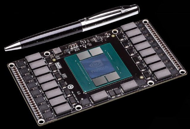
NVIDIA's next-generation GPUs, based on the company's "Pascal" architecture, will be reportedly built on the 16 nanometer FinFET node at TSMC, and not the previously reported 14 nm FinFET node at Samsung. Talks of foundry partnership between NVIDIA and Samsung didn't succeed, and the GPU maker decided to revert to TSMC. The "Pascal" family of GPUs will see NVIDIA adopt HBM2 (high-bandwidth memory 2), with stacked DRAM chips sitting alongside the GPU die, on a multi-chip module, similar to AMD's pioneering "Fiji" GPU. Rival AMD, on the other hand, could build its next-generation GCNxt GPUs on 14 nm FinFET process being refined by GlobalFoundries.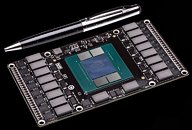
Source:
BusinessKorea
52 Comments on NVIDIA "Pascal" GPUs to be Built on 16 nm TSMC FinFET Node