Wednesday, January 30th 2019

AMD Updates Wafer Supply Agreement with GlobalFoundries to Free Itself of "7nm Tax"
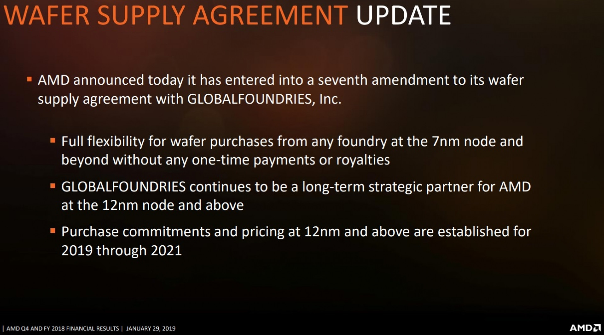
AMD in its Q4-2018 Earnings Report disclosed that it has amended its Wafer Supply Agreement (WSA) with GlobalFoundries that frees it from paying a "7 nanometer tax." Under the older version of WSA, AMD would have had to pay a penalty to GlobalFoundries if it sourced processors from any other semiconductor foundry. The company got preferential pricing in return for the exclusivity. With GlobalFoundries discontinuing development of cutting-edge processes such as 7 nm and 5 nm, it makes sense for AMD to seek out other foundry partners, such as TSMC, and an amendment to the WSA was needed. With this amendment in place, AMD can go ahead and source 7 nm dies from TSMC without paying penalties to GlobalFoundries (GloFo).
With its "Zen 2" microarchitecture, AMD is going big on multi-chip modules, in which only those components that can tangibly benefit from the switch to the 7 nm node, namely the CPU cores, would be built on 7 nm dies, called "CPU chiplets," while components that don't need the miniaturization just yet, such as the processor's memory controller, PCIe root-complex, etc., will be built on separate dies called "I/O controllers." These dies will continue to be 14 nm, and likely supplied by GloFo. Final packaging of 7 nm CPU chiplets from TSMC, and 14 nm I/O controllers from GloFo, will happen at GloFo's facilities in China or Malaysia. AMD in its amendment committed to purchasing 14 nm and 12 nm chips from GloFo between 2019 and 2021, which means the MCM approach to processors is here to stay.
Source:
Overclock3D
With its "Zen 2" microarchitecture, AMD is going big on multi-chip modules, in which only those components that can tangibly benefit from the switch to the 7 nm node, namely the CPU cores, would be built on 7 nm dies, called "CPU chiplets," while components that don't need the miniaturization just yet, such as the processor's memory controller, PCIe root-complex, etc., will be built on separate dies called "I/O controllers." These dies will continue to be 14 nm, and likely supplied by GloFo. Final packaging of 7 nm CPU chiplets from TSMC, and 14 nm I/O controllers from GloFo, will happen at GloFo's facilities in China or Malaysia. AMD in its amendment committed to purchasing 14 nm and 12 nm chips from GloFo between 2019 and 2021, which means the MCM approach to processors is here to stay.
13 Comments on AMD Updates Wafer Supply Agreement with GlobalFoundries to Free Itself of "7nm Tax"
Epcy, Ryzen 3000 series & Navi margins 38-41%
AMD with it's large orders gives them higher priority over NVIDIA at TSMC Rome is 8 chips alone Ryzen 3000 series 2 chips.
AMD didn't want to do two foundries, when they could do it on one fab. Which foundry T will have better volume than that of Globalfoundries for the 7nm 193i and 7nm EUV nodes.
12FDX seems to have a practical limit @150mm², but this is all well documented and plus AMD is the king of semi-custom, amirite?
28nm -> 22FDX -> 12FDX with large dies are completely okay. Rather than going 28nm bulk -> 20nm planar bulk -> 14nm planar bulk, etc.
22FDX's limit compared to FinFETs is around 180 mm squared.
12FDX's limit compared to FinFETs is around 270 mm squared.
With the most current version of the FEOL/MOL/BEOL.
If channel mobility goes up, so does drive current.
Why FDSOI and FinFET don't go together. Is that those that went FinFET have already designed around FinFET's issues. However those that are going FDSOI route, will simply bypass FinFETs all together.
FDSOI => Lower cost, lower development time, more cool/less power, etc.
FinFET => Higher cost, longer development time, more hot/higher power, etc.
Going both requires big pockets.
A pure FDSOI chiplet design is better for power.
A pure FinFET chiplet design is better for performance.
A mixed FDSOI+FinFET chiplet design requires FinFET development time and FinFET cost.
CEOat IBM who is the currentCEO"CTO" at GF directly challenged the board at IBM when they greenlighted '7nm' and I don't think he erred on the point:- 7nm is 3 times more expensive which is what bankrupted IBM's foundry business,
- 12nm is not that much more expensive than 14nm,
- A cross development between FDX and FinFET is bound to be expensive, but remember the CEO who is at play here, he does not want 7nm!
I think I might have a point here if not mistaken.*PS: I'll have to check whether it was just '7nm' singularly or '7nm FinFET' that they were aiming for at the time, but out the top of my mind I think it was 7nm FinFETs.