Friday, December 6th 2019

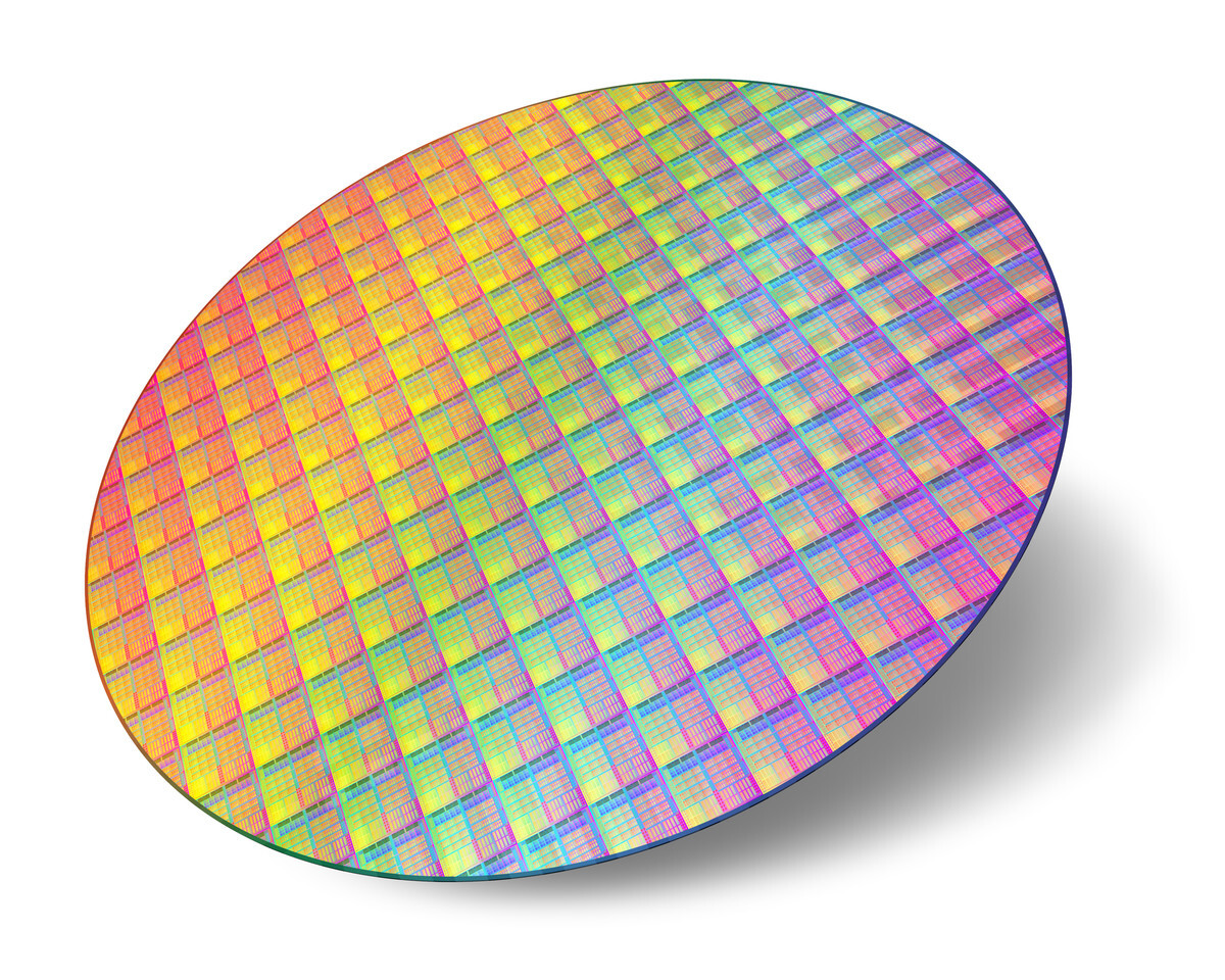
TSMC on Track to Deliver 3 nm in 2022
TSMC is delivering record results day after day, with a 5 nm manufacturing process starting High Volume Manufacturing (HVM) in Q2 next year, 7 nm process getting plenty of orders and the fact that TSMC just became the biggest company publicly trading in Asia. Continuing with the goal to match or even beat the famous Moore's Law, TSMC is already planning for future 3 nm node manufacturing, promised to start HVM as soon as 2022 arrives, according to JK Wang, TSMC's senior vice president of fab operations. Delivering 3 nm a whole year before originally planned in 2023, TSMC is working hard, with fab construction work doing quite well, judging by all the news that the company is releasing recently.
We can hope to see the first wave of products built using 3 nm manufacturing process sometime around end of year 2022, when the holiday season arrives. Usual customers like Apple and HiSilicon will surely utilize the new node and deliver their smartphones with 3 nm processors inside as soon as the process is ready for HVM.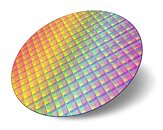
Source:
DigiTimes
We can hope to see the first wave of products built using 3 nm manufacturing process sometime around end of year 2022, when the holiday season arrives. Usual customers like Apple and HiSilicon will surely utilize the new node and deliver their smartphones with 3 nm processors inside as soon as the process is ready for HVM.
71 Comments on TSMC on Track to Deliver 3 nm in 2022
Intel is going to find out the same way in a few years.
But from 7nm to 6nm just 1.18x, even if TSMC keeps releasing new nodes the improvement between one and the next is every time lesser.
Hipsters. Definitely *performs Fortnite dance*
(/s) ;)
Somewhat unrelated, but it's also what will most likely make weird for Intel, when their 7nm node will be ready shortly after they figure out 10nm.
And it's going to be a blast about 5 years from now when everybody hits the physical limits of Si and we all get stuck on 2 or 3nm, while fabs shrink various parts of the transistor. If you think 14nm+++++ was embarrassing, just wait for 3nm++++++++++++++ :D
We can’t go much smaller AFAIK at least with silicon, but it’s lasted longer than anticipated. What’s on the horizon and how do you overcome hard quantum limits. The process can’t get arbitrarily small, atoms are about 0.1nm for the the simplest ones. Imagine line traces so small only a single electron at a time can pass, but they could never be made that small.
Also, Tencent called and said that Fiftycent is stealing their lunch ever day at school.