Friday, October 25th 2019

TSMC Begins 3 nm Fab Construction

TSMC has been very aggressive with its approach to silicon manufacturing, with more investments into its R&D that now match or beat the capex investments of Intel. That indicates a strong demand for new technologies and TSMC's strong will not drop out of the never-ending race for more performance and smaller node sizes.

According to the sources over at DigiTimes, TSMC has acquired as much as 30 hectares of land in the Southern Taiwan Science Park to begin the construction of its fabs that are supposed to start high-volume manufacturing 3 nm node in 2023. Construction of 3 nm manufacturing facilities are set to begin in 2020 when TSMC will lay the groundwork for the new fab. The 3 nm semiconductor node is expected to be TSMC's third attempt at EUV lithography, right after the 7 nm+, and 5 nm nodes which are also based on EUV technology.
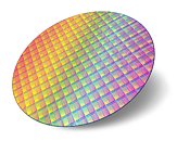
Source: DigiTimes
Add your own comment

19 Comments on TSMC Begins 3 nm Fab Construction

#2
Space Lynx
Astronaut
really amazing how fast it is all moving.
Posted on Reply
#3
micropage7
3nm for this year?
While i still run 14nm
Posted on Reply
#4
ShurikN
micropage73nm for this year?
While i still run 14nm
No mate XD
Facilities are being built from 2020, and the silicon will come out in 2023
Posted on Reply
#5
ppn
Zen radeon ps5 shrinks in 2023 + 2 yrs. I would hold any major upgrade until 2nm++ is available.
Posted on Reply
#6
GeorgeMan
After 1nm what are we gonna do??
Posted on Reply
#8
kapone32
Well at least we know we will be getting real node upgrades from AMD for at least the next 4 years.
GeorgeManAfter 1nm what are we gonna do??
By that time PCs will be good enough for us to build a poor man's rocket and use the computer to guide us to the moon and back :) Oh wait we can already do that.
Posted on Reply
#9
euricog
GeorgeManAfter 1nm what are we gonna do??
If only we could represent a number higher than zero and lower than 1... maybe we find a way some 0.94 decades from now...
Posted on Reply
#10
AleksandarK
News Editor
GeorgeManAfter 1nm what are we gonna do??
Read this
Posted on Reply
#11
sam_86314
GeorgeManAfter 1nm what are we gonna do??
There's probably some hard limit that isn't too far away. A water molecule is about 270 picometers or 0.27 nm wide.
Posted on Reply
#12
euricog
From TPU's editorial linked by @AleksandarK: "Moore's Law - Is it Really Dead ?":
And last but not the least is the 3rd dimension. When we step below 1 nm and start measuring node size in picometers, many forces will prevent transistors from getting smaller. You can go small but you can't break the rules of physics. Quantum tunneling is more present at smaller distances, so at one point we can not go smaller in design without having the transistor make the switch at random times. So when we hit the limits, there is still one place where transistors can be put and that is the vertical axis. If we stack transistors on top of each other, we can automatically double, triple or even quadruple the number of transistors per square millimeter, making the potential of this approach quite big. We already use this technology on HBM memory, and it is about to transfer to logic as well. TSMC also makes Wafer-on-Wafer packages which allow for stacking wafers on top of each other, so it isn't impossible to go 3D and pack more performance in same area, but heat, especially heat density can become a problem.
Posted on Reply
#13
Keemzay
micropage73nm for this year?
While i still run 14nm
you guys are running 14nm? (have 22nm)
Posted on Reply
#14
voltage
GeorgeManAfter 1nm what are we gonna do??
0 -1 -2 -3 etc...
Posted on Reply
#15
R-T-B
voltage0 -1 -2 -3 etc...
Or you could just you know, use the next unit down on the metric scale (picometre), like last time (we switched from micrometeres not that far ago).
Posted on Reply
#17
64K
I wonder how small we can go and still produce the chips cheaply enough so that they are affordable to use.
Posted on Reply
#18
quadibloc
GeorgeManAfter 1nm what are we gonna do??
Obviously, if there is a next generation after that - and I'm not sure we can go lower than even 3nm - it would be 700 pm. Then 500 pm, 300 pm, 200 pm, 150 pm, 100 pm, 70 pm... . And after 1 picometre, there's always femtometres.
Posted on Reply
#19
Space Lynx
Astronaut
IBM has not given up on carbon nanotubes replacing silicon someday, so silicon and nanometers may be a thing of the past someday anyway, i mean its still a fantasy right now, but they have made some progress I read earlier this year
Posted on Reply
Add your own comment
Apr 25th, 2024 05:42 EDT change timezone

New Forum Posts

Popular Reviews

Controversial News Posts