Thursday, May 14th 2020

NVIDIA Ampere A100 Has 54 Billion Transistors, World's Largest 7nm Chip

Not long ago, Intel's Raja Koduri claimed that the Xe HP "Ponte Vecchio" silicon was the "big daddy" of Xe GPUs, and the "largest chip co-developed in India," larger than the 35 billion-transistor Xilinix VU19P FPGA co-developed in the country. It turns out that NVIDIA is in the mood for setting records. The "Ampere" A100 silicon has 54 billion transistors crammed into a single 7 nm die (not counting transistor counts of the HBM2E memory stacks).

NVIDIA claims a 20 Times boost in both AI inference and single-precision (FP32) performance over its "Volta" based predecessor, the Tesla V100. The chip also offers a 2.5X gain in FP64 performance over "Volta." NVIDIA has also invented a new number format for AI compute, called TF32 (tensor float 32). TF32 uses 10-bit mantissa of FP16, and the 8-bit exponent of FP32, resulting in a new, efficient format. NVIDIA attributes its 20x performance gains over "Volta" to this. The 3rd generation tensor core introduced with Ampere supports FP64 natively. Another key design focus for NVIDIA is to leverage the "sparsity" phenomenon in neural nets, to reduce their size, and improve performance.
A new HPC-relevant feature being introduced with A100 is multi-instance GPU, which allows multiple complex applications to run on the same GPU without sharing resources such as memory bandwidth. The user can now partition a physical A100 into up to 7 virtual GPUs of varying specs, and ensure that an application running on one of the vGPUs doesn't eat into the resources of the other. As for real-world performance, NVIDIA claims that the A100 beat the V100 by a factor of 7 at BERT.

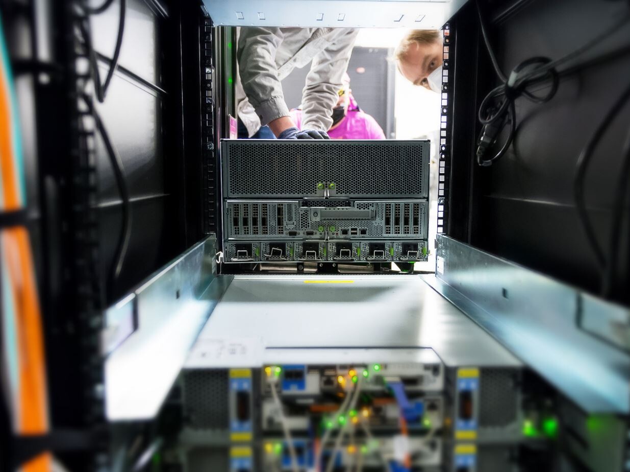
The DGX-A100 system crams 5 petaflops of compute peformance onto a single "graphics card" (a single node), and starts at $199,000 a piece.
Sources: VideoCardz, EETimes
Add your own comment

20 Comments on NVIDIA Ampere A100 Has 54 Billion Transistors, World's Largest 7nm Chip

#1
Fluffmeister
Wowzers, this bad boy is going to get a lot of love in HPC market.
Posted on Reply
#2
Vya Domus
NVIDIA will also invent a new number format for AI compute, called TF32 (tensor float 32). TF32 uses 10-bit mantissa of FP16, and the 8-bit exponent of FP32
Wouldn't that be ... TF19 ? 10 + 8 + 1 (sign) bits
Posted on Reply
#4
theGryphon
FluffmeisterWowzers, this bad boy is going to get a lot of love in HPC market.
Had the exact same reaction as I was reading...
Posted on Reply
#5
londiste
54B transistors is three times as much as TU102 (18.6B, Titan RTX, RTX2080Ti). Volta has 21.1B.
Posted on Reply
#6
renz496
so what it's exact FP32/64 performance?
Posted on Reply
#7
Vya Domus
renz496so what it's exact FP32/64 performance?
My guess around 30 TFLOPS FP32, this probably has about twice the shaders of V100 but probably no where the clock speed.
Posted on Reply
#8
agentnathan009
Ampere to Ponte Vecchio, “who’s your daddy now?”
Posted on Reply
#9
R0H1T
How about Zen4 (or 5?) with upto 128 real cores :nutkick:
Posted on Reply
#10
ironcerealbox
Vya DomusWouldn't that be ... TF19 ? 10 + 8 + 1 (sign) bits
Yar? Yar!

Good catch! I noticed it too.

However, what's really going on is that they are creating their own alternative to BF16 (brainfloat16) and calling it TF32: keeping the 8 bits for exponent from fp32 but using only 10 bits for the fraction (precision) from fp16. This keeps the approximate range of FP32 while keeping the precision of FP16 (half precision). This is different than BF16 since BF16 only keeps 7 bits for precision. So, you can get better (or what some of my students say..."gooder") approximations with TF32 when converting back to FP32 (by padding the last 13 bits of precision on FP32 with zeroes) instead of with BF16 (where you would pad the last 16 bits with zeroes).

Does it really matter that much in the end? I'm not a professional with experience in AIs or DNNs but I suppose that FP32 approximations from TF32 is better and only ever so slightly slower than FP32 approximations from BF16. It is somewhat clever with what they did.

But, back to the whole TF19 bit (no pun intended!): I think it's a marketing move as TF32 "sounds" better. It's really TF19 with 1 bit sign, 8 bit exponent, and 10 bit fraction but, hey, "TF32" FTW.
Vya DomusMy guess around 30 TFLOPS FP32, this probably has about twice the shaders of V100 but probably no where the clock speed.
7FF+ is supposedly on par with clock speeds or slightly better than 12FF. If it is indeed 8192 cores, then we'd have around 29.5 TFLOPS to 32.8 TFLOPS (1.8 GHz to 2 GHz, respectively). "TF32" could be as high as 655.4 TFLOPS, or, if one has a cool $200K lying around, you can get that monstrosity that JSH has been baking and get 8x 655.4 TFLOPS = 5.243 PFLOPS of "TF32" performance. I mean...saying PFLOPS like "Pee-Flops" is just ridiculous...

Aaaaaaand...I'm getting off topic.
Posted on Reply
#11
Aquinus
Resident Wat-man
Hah! Yields are probably as good as winning the lottery. Does nVidia really think that going this direction is a good idea? Huge monolithic dies are such a waste of resources because yields are abysmal. I guess that's okay when a business is willing to spend whatever it takes to have a leg up. Personally, I think that until we start seeing MCM solutions to compute scaling, I'm reluctant to believe that any gains are going to be substantial or long lasting in this market.

tl;dr: Big dies are not the answer.
Posted on Reply
#12
Fluffmeister
agentnathan009Ampere to Ponte Vecchio, “who’s your daddy now?”
Heh, and finally we see a chip worthy of "Poor Volta" too.
Posted on Reply
#13
ironcerealbox
AquinusHah! Yields are probably as good as winning the lottery. Does nVidia really think that going this direction is a good idea? Huge monolithic dies are such a waste of resources because yields are abysmal. I guess that's okay when a business is willing to spend whatever it takes to have a leg up. Personally, I think that until we start seeing MCM solutions to compute scaling, I'm reluctant to believe that any gains are going to be substantial or long lasting in this market.

tl;dr: Big dies are not the answer.
Their [Nvidia] next architecture is Hopper and it is confirmed to be their first using MCMs. Hell, it might be the only thing confirmed about Hopper.
Posted on Reply
#14
midnightoil
FluffmeisterWowzers, this bad boy is going to get a lot of love in HPC market.
You're forgetting that the big boys in HPC already know pretty much what AMD / NVIDIA / Intel have in the pipeline for the next 2 gens.

AMD have been scooping most of the biggest contracts lately, and most of the really big contracts in the last 18 months have been aiming at CDNA2 / Hopper, not Ampere or CDNA1.

That 20x figure is pure fantasy land.
Posted on Reply
#15
Vya Domus
midnightoilThat 20x figure is pure fantasy land.
I wouldn't necessarily say that. They're changing the metric, they've done it before with "gigarays", it's the good old " We're faster ! " *with an asterisk* .
midnightoilYou're forgetting that the big boys in HPC already know pretty much what AMD / NVIDIA / Intel have in the pipeline for the next 2 gens.
That's true and it's telling, if they still decided to go with AMD it shows that maybe they're weren't as impressed with what Nvidia was about to have.
ironcerealbox7FF+ is supposedly on par with clock speeds or slightly better than 12FF.
The problem isn't that it couldn't clock, it's power. V100 runs at 1400Mhz but this has more than twice the transistors, if they want to maintain the 250W power envelope it's just not possible to have it run at the same clock speed.
AquinusHah! Yields are probably as good as winning the lottery. Does nVidia really think that going this direction is a good idea? Huge monolithic dies are such a waste of resources because yields are abysmal. I guess that's okay when a business is willing to spend whatever it takes to have a leg up. Personally, I think that until we start seeing MCM solutions to compute scaling, I'm reluctant to believe that any gains are going to be substantial or long lasting in this market.

tl;dr: Big dies are not the answer.
I find this exceedingly strange too. These 800 mm^2 dies are going to be insanely expensive and so will be the actual products, I think businesses are willing to spend up to a point. With more and more dedicated silicon out there for inferencing/training I don't think Nvidia is in a position to ask even more money for something that people can get else were for a fraction of the cost. They are optimizing their chips for too many things, some time ago that used to be an advantage but it's slowly becoming an Achilles heel.
Posted on Reply
#16
xkm1948
FluffmeisterWowzers, this bad boy is going to get a lot of love in HPC market.
Exactly.

Also i find it really funny that so many "home grown HPC experts" suddenly show up here claiming CDNA2 or whatever made-up crap.

HPC is all about ecosystem where both software and hardware are needed in excellent shape. Pay attention to how much Nvidia CEO acknowledged the software developers. Without a thriving software ecosystem, the hardware by themselves are nothing. In the field of AI, nobody is currently able to compete with Nvidia's software and hardware integration.

Computing hardware is only half (Hell, actually 1/3) of the deal. There is software which is a HUGE part, as well as inter-connecting hardware.
Posted on Reply
#17
midnightoil
The contracts are already published.

Get a clue.
Posted on Reply
#18
Yosar
xkm1948HPC is all about ecosystem where both software and hardware are needed in excellent shape. Pay attention to how much Nvidia CEO acknowledged the software developers. Without a thriving software ecosystem, the hardware by themselves are nothing. In the field of AI, nobody is currently able to compete with Nvidia's software and hardware integration.

Computing hardware is only half (Hell, actually 1/3) of the deal. There is software which is a HUGE part, as well as inter-connecting hardware.
If you pay millions of dollars for hardware, you also pay for _specialized_ software for this hardware. You surely don't buy hardware for 200 000 dollars (for 1 card) to run 3DS MAX Studio. Your eco-system doesn't matter. This whole hardware is your eco-system. The deal is for eco-system.
Posted on Reply
#19
R-T-B
AquinusHah! Yields are probably as good as winning the lottery. Does nVidia really think that going this direction is a good idea? Huge monolithic dies are such a waste of resources because yields are abysmal. I guess that's okay when a business is willing to spend whatever it takes to have a leg up. Personally, I think that until we start seeing MCM solutions to compute scaling, I'm reluctant to believe that any gains are going to be substantial or long lasting in this market.

tl;dr: Big dies are not the answer.
They are when the customer is willing to pay top dollar, like HPC.
Posted on Reply
#20
Aquinus
Resident Wat-man
R-T-BThey are when the customer is willing to pay top dollar, like HPC.
I think that depends on what the alternatives cost and how easy or hard it is to build the software to work on any of the HPC solutions a business might be considering. None of this changes the fact though that a massive die like this is going to put a huge premium on the hardware, which means less money for the other things that also matter. What good is great hardware if you have to skimp on the software side of things?
Posted on Reply
Add your own comment
Jun 14th, 2024 19:43 EDT change timezone

New Forum Posts

Popular Reviews

Controversial News Posts