News Posts matching #Tesla V100

Return to Keyword Browsing

TOP500: Frontier Keeps Top Spot, Aurora Officially Becomes the Second Exascale Machine

The 63rd edition of the TOP500 reveals that Frontier has once again claimed the top spot, despite no longer being the only exascale machine on the list. Additionally, a new system has found its way into the Top 10.

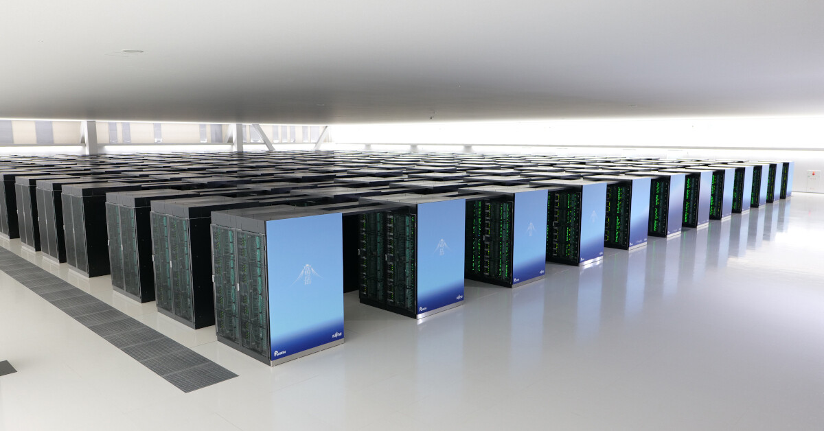
The Frontier system at Oak Ridge National Laboratory in Tennessee, USA remains the most powerful system on the list with an HPL score of 1.206 EFlop/s. The system has a total of 8,699,904 combined CPU and GPU cores, an HPE Cray EX architecture that combines 3rd Gen AMD EPYC CPUs optimized for HPC and AI with AMD Instinct MI250X accelerators, and it relies on Cray's Slingshot 11 network for data transfer. On top of that, this machine has an impressive power efficiency rating of 52.93 GFlops/Watt - putting Frontier at the No. 13 spot on the GREEN500.

TOP500 Update: Frontier Remains No.1 With Aurora Coming in at No. 2

The 62nd edition of the TOP500 reveals that the Frontier system retains its top spot and is still the only exascale machine on the list. However, five new or upgraded systems have shaken up the Top 10.

Housed at the Oak Ridge National Laboratory (ORNL) in Tennessee, USA, Frontier leads the pack with an HPL score of 1.194 EFlop/s - unchanged from the June 2023 list. Frontier utilizes AMD EPYC 64C 2GHz processors and is based on the latest HPE Cray EX235a architecture. The system has a total of 8,699,904 combined CPU and GPU cores. Additionally, Frontier has an impressive power efficiency rating of 52.59 GFlops/watt and relies on HPE's Slingshot 11 network for data transfer.

Frontier Remains As Sole Exaflop Machine on TOP500 List

Increasing its HPL score from 1.02 Eflop/s in November 2022 to an impressive 1.194 Eflop/s on this list, Frontier was able to improve upon its score after a stagnation between June 2022 and November 2022. Considering exascale was only a goal to aspire to just a few years ago, a roughly 17% increase here is an enormous success. Additionally, Frontier earned a score of 9.95 Eflop/s on the HLP-MxP benchmark, which measures performance for mixed-precision calculation. This is also an increase over the 7.94 EFlop/s that the system achieved on the previous list and nearly 10 times more powerful than the machine's HPL score. Frontier is based on the HPE Cray EX235a architecture and utilizes AMD EPYC 64C 2 GHz processors. It also has 8,699,904 cores and an incredible energy efficiency rating of 52.59 Gflops/watt. It also relies on gigabit ethernet for data transfer.

ORNL's Exaflop Machine Frontier Keeps Top Spot, New Competitor Leonardo Breaks the Top10 List

The 60th edition of the TOP500 reveals that the Frontier system is still the only true exascale machine on the list.

With an HPL score of 1.102 EFlop/s, the Frontier machine at Oak Ridge National Laboratory (ORNL) did not improve upon the score it reached on the June 2022 list. That said, Frontier's near-tripling of the HPL score received by second-place winner is still a major victory for computer science. On top of that, Frontier demonstrated a score of 7.94 EFlop/s on the HPL-MxP benchmark, which measures performance for mixed-precision calculation. Frontier is based on the HPE Cray EX235a architecture and it relies on AMD EPYC 64C 2 GHz processor. The system has 8,730,112 cores and a power efficiency rating of 52.23 gigaflops/watt. It also relies on gigabit ethernet for data transfer.

TOP500 Update Shows No Exascale Yet, Japanese Fugaku Supercomputer Still at the Top

The 58th annual edition of the TOP500 saw little change in the Top10. The Microsoft Azure system called Voyager-EUS2 was the only machine to shake up the top spots, claiming No. 10. Based on an AMD EPYC processor with 48 cores and 2.45GHz working together with an NVIDIA A100 GPU and 80 GB of memory, Voyager-EUS2 also utilizes a Mellanox HDR Infiniband for data transfer.

While there were no other changes to the positions of the systems in the Top10, Perlmutter at NERSC improved its performance to 70.9 Pflop/s. Housed at the Lawrence Berkeley National Laboratory, Perlmutter's increased performance couldn't move it from its previously held No. 5 spot.

TOP500 Expands Exaflops Capacity Amidst Low Turnover

The 56th edition of the TOP500 saw the Japanese Fugaku supercomputer solidify its number one status in a list that reflects a flattening performance growth curve. Although two new systems managed to make it into the top 10, the full list recorded the smallest number of new entries since the project began in 1993.

The entry level to the list moved up to 1.32 petaflops on the High Performance Linpack (HPL) benchmark, a small increase from 1.23 petaflops recorded in the June 2020 rankings. In a similar vein, the aggregate performance of all 500 systems grew from 2.22 exaflops in June to just 2.43 exaflops on the latest list. Likewise, average concurrency per system barely increased at all, growing from 145,363 cores six months ago to 145,465 cores in the current list.

NVIDIA Ampere A100 Has 54 Billion Transistors, World's Largest 7nm Chip

Not long ago, Intel's Raja Koduri claimed that the Xe HP "Ponte Vecchio" silicon was the "big daddy" of Xe GPUs, and the "largest chip co-developed in India," larger than the 35 billion-transistor Xilinix VU19P FPGA co-developed in the country. It turns out that NVIDIA is in the mood for setting records. The "Ampere" A100 silicon has 54 billion transistors crammed into a single 7 nm die (not counting transistor counts of the HBM2E memory stacks).

NVIDIA claims a 20 Times boost in both AI inference and single-precision (FP32) performance over its "Volta" based predecessor, the Tesla V100. The chip also offers a 2.5X gain in FP64 performance over "Volta." NVIDIA has also invented a new number format for AI compute, called TF32 (tensor float 32). TF32 uses 10-bit mantissa of FP16, and the 8-bit exponent of FP32, resulting in a new, efficient format. NVIDIA attributes its 20x performance gains over "Volta" to this. The 3rd generation tensor core introduced with Ampere supports FP64 natively. Another key design focus for NVIDIA is to leverage the "sparsity" phenomenon in neural nets, to reduce their size, and improve performance.

Huawei Rumored To Enter GPU Server Market

Huawei may become the 4th player in the GPU server market if a new report by Korean news outlet The Elec is to be believed. The Elec has received reports from Industry Sources that Huawei is readying to enter the market in 2020, this will put them in direct competition with industry leader NVIDIA along with AMD and newcomer Intel. Huawei Korea will reportedly assign the project to the new Cloud and AI Business Group division, talent scouting has already begun with rumors of current and former NVIDIA staff getting poached.

Huawei is no newcomer to the server market having already launched the Ascend 910 one of the worlds most advanced AI accelerators in August 2019. The Ascend 910 outperforms the Tesla V100 by a factor of two, and is developed on a more advanced 7 nm+ technology compared to the 12 nm Tesla V100. In January 2020 Huawei launched their next server product the Kunpeng 920 a big data CPU along with a new server lineup featuring the chip. Considering Huawei's experience and resources in the server market along with Intel's entrance the GPU server landscape is set to become very competitive.

EK Water Blocks Unveils EK-FC GV100 Pro, A Water Block for Professionals

EK Water Blocks, the premium computer liquid cooling gear manufacturer, is releasing a workstation/server grade water block for some of the most powerful Workstation GPUs on the market today based on the NVIDIA GV100 graphic chip. That includes both the Quadro GV100 and Tesla V100, as well as the Titan V. The EK-FC GV100 Pro water block spans across the entire length of the card cooling all critical components.

With the launch of this water block, its clear that EKs plan of expansion into the professional workstation and server grade market is well under way. In the following months you can expect many more worksation and enterprise cooling solutions from EK.

ASUS Introduces Full Lineup of PCI-E Servers Powered by NVIDIA Tesla GPUs

ASUS, the leading IT Company in server systems, server motherboards, workstations and workstation motherboards, today announced support for the latest NVIDIA AI solutions with NVIDIA Tesla V100 Tensor Core 32GB GPUs and Tesla P4 on its accelerated computing servers.
Artificial intelligence (AI) is translating data into meaningful insights, services and scientific breakthroughs. The size of the neural networks powering this AI revolution has grown tremendously. For instance, today's state of the art neural network model for language translation, Google's MOE model has 8 billion parameters compared to 100 million parameters of models from just two years ago.

To handle these massive models, NVIDIA Tesla V100 offers a 32GB memory configuration, which is double that of the previous generation. Providing 2X the memory improves deep learning training performance for next-generation AI models by up to 50 percent and improves developer productivity, allowing researchers to deliver more AI breakthroughs in less time. Increased memory allows HPC applications to run larger simulations more efficiently than ever before.

TechPowerUp Releases GPU-Z v2.9.0

TechPowerUp today released GPU-Z v2.9.0, the latest version of the graphics sub-system information, diagnostic, and monitoring utility no enthusiast can leave home without. Version 2.9.0 fixes some of the bugs encountered with Windows 10 April 2018 Update, with support for new WDDM 2.4 drivers. Support is also added for NVIDIA Tesla V100, and NVIDIA GPUs in TCC mode (eg: Tesla and Quadro families). Also added is support for "Haswell" GT1 variant (found on certain Celeron SKUs), and more AMD "Bristol Ridge" APU graphics variants.

At AMD's request, we disabled "Vega" SoC clock and hot-spot sensors by default. You can manually enable them any time in the settings. For enthusiasts who have GPU-Z launched at start-up (as a Scheduled Task), Windows will no longer nag with the "this file was downloaded from the Internet" dialog every time. PerfCap reason for Tesla GPUs in TCC mode has been fixed to "none." Detection of various AMD "Carrizo," "Bristol Ridge" and "Stoney Ridge" GPUs were fixed. The overall drawing code for the sensor graphs is improved. Grab GPU-Z from the link below.
DOWNLOAD: TechPowerUp GPU-Z 2.9.0

The Change-log follows.

NVIDIA Announces the DGX-2 System - 16x Tesla V100 GPUs, 30 TB NVMe Memory for $400K

NVIDIA's DGX-2 is likely the reason why NVIDIA seems to be slightly less enamored with the consumer graphics card market as of late. Let's be honest: just look at that price-tag, and imagine the rivers of money NVIDIA is making on each of these systems sold. The data center and deep learning markets have been pouring money into NVIDIA's coffers, and so, the company is focusing its efforts in this space. Case in point: the DGX-2, which sports performance of 1920 TFLOPs (Tensor processing); 480 TFLOPs of FP16; half again that value at 240 TFLOPs for FP32 workloads; and 120 TFLOPs on FP64.

NVIDIA's DGX-2 builds upon the original DGX-1 in all ways thinkable. NVIDIA looks at these as readily-deployed processing powerhouses, which include everything any prospective user that requires gargantuan amounts of processing power can deploy in a single system. And the DGX-2 just runs laps around the DGX-1 (which originally sold for $150K) in all aspects: it features 16x 32GB Tesla V100 GPUs (the DGX-1 featured 8x 16 GB Tesla GPUs); 1.5 TB of system ram (the DGX-1 features a paltry 0.5 TB); 30 TB NVMe system storage (the DGX-1 sported 8 TB of such storage space), and even includes a pair of Xeon Platinum CPUs (admittedly, the lowest performance increase in the whole system).

HWiNFO Adds Support For Upcoming AMD CPUs, GPUs, Others

PC diagnostics tool HW Info has added support for future, as-of-yet unreleased AMD CPUs and GPUs, which seemingly confirm some earlier news on AMD's plans for their next-generation offerings. HWiNFO's v5.72 update adds support for upcoming AMD Navi GPUs, Pinnacle Ridge, 400-series motherboards (which should make their market debut alongside AMD's Zen+ CPUs), and enhanced support for AMD's Starship, Matisse and Radeon RX Vega M. We already touched upon AMD's Matisse codename in the past: it's expected to refer to the company's Zen 2 microarchitecture, which will bring architecture overhauls of the base Zen design - alongside a 7 nm process - in order to bring enhanced performance and better power consumption.

Starship, on the other hand, is a previously leaked evolution of AMD's current Naples offering that powers their EPYC server CPUs. Starship has been rumored to have been canceled, and then put back on the product schedule again; if anything, its inclusion in HWiNFO's latest version does point towards it having made the final cut, after all. Starship will bring to businesses an increased number of cores and threads (48/96) compared to Naples' current top-tier offering (32/64), alongside a 7 nm manufacturing process.

NVIDIA Quadro GV100 Surfaces in Latest NVFlash Binary

NVIDIA could be giving final touches to its Quadro GV100 "Volta" professional graphics card, after the surprise late-2017 launch of the NVIDIA TITAN V. The card was found listed in the binary view of the latest version of NVFlash (v5.427.0), the most popular NVIDIA graphics card BIOS extraction and flashing utility. Since its feature-set upgrade to the TITAN Xp through newer drivers, NVIDIA has given the TITAN family of graphics cards a quasi-professional differentiation from its GeForce GTX family.

The Quadro family still has the most professional features, software certifications, and are sought after by big companies into graphics design, media, animation, architecture, resource exploration, etc. The Quadro GV100 could hence yet be more feature-rich than the TITAN V. With its GV100 silicon, NVIDIA is using a common ASIC and board design for its Tesla V100 PCIe add-in card variants, the TITAN V, and the Quadro GV100. While the company endowed the TITAN V with 12 GB of HBM2 memory using 3 out of 4 memory stacks the ASIC is capable of holding; there's an opportunity for NVIDIA to differentiate the Quadro GV100 by giving it that 4th memory stack, and 16 GB of total memory. You can download the latest version of NVFlash here.

NVIDIA TITAN V Lacks SLI or NVLink Support

Earlier today, we brought you a story about NVIDIA TITAN V setting you back by up to $7,196 for two cards and two $600 NVLink cables. We got word from NVIDIA that the card neither features NVLink, nor supports SLI, and have since edited it. The NVLink fingers on the TITAN V card are rudiments of the functional NVLink interface found on the Tesla V100 PCIe, being developed by NVIDIA, as the TITAN V, Tesla V100, and a future Quadro GV100 share a common PCB. The NVLink fingers on the TITAN V are concealed by the base-plate of the cooler on one side, and the card's back-plate on the other; so the female connectors of NVLink bridge cables can't be plugged in.

With the lack of SLI support on what is possibly it's fastest graphics card based on the "Volta" architecture, NVIDIA seems to have responded to market trends that multi-GPU is dying or dead. That said, it would be interesting to see if professional overclockers chasing benchmark leaderboard glory pick up the TITAN V, as opposed to two TITAN Xp in SLI or four Radeon RX Vega 64 in 4-way CrossFireX.

NVIDIA Announces TITAN V "Volta" Graphics Card

NVIDIA in a shock move, announced its new flagship graphics card, the TITAN V. This card implements the "Volta" GV100 graphics processor, the same one which drives the company's Tesla V100 HPC accelerator. The GV100 is a multi-chip module, with the GPU die and three HBM2 memory stacks sharing a package. The card features 12 GB of HBM2 memory across a 3072-bit wide memory interface. The GPU die has been built on the 12 nm FinFET+ process by TSMC. NVIDIA TITAN V maxes out the GV100 silicon, if not its memory interface, featuring a whopping 5,120 CUDA cores, 640 Tensor cores (specialized units that accelerate neural-net building/training). The CUDA cores are spread across 80 streaming multiprocessors (64 CUDA cores per SM), spread across 6 graphics processing clusters (GPCs). The TMU count is 320.

The GPU core is clocked at 1200 MHz, with a GPU Boost frequency of 1455 MHz, and an HBM2 memory clock of 850 MHz, translating into 652.8 GB/s memory bandwidth (1.70 Gbps stacks). The card draws power from a combination of 6-pin and 8-pin PCIe power connectors. Display outputs include three DP and one HDMI connectors. With a wallet-scorching price of USD $2,999, and available exclusively through NVIDIA store, the TITAN V is evidence that with Intel deciding to sell client-segment processors for $2,000, it was a matter of time before GPU makers seek out that price-band. At $3k, the GV100's margins are probably more than made up for.

Supermicro Releases Supercharged NVIDIA Volta Systems

Super Micro Computer, Inc. (NASDAQ: SMCI), a global leader in enterprise computing, storage, and networking solutions and green computing technology, today announced support for NVIDIA Tesla V100 PCI-E and V100 SXM2 GPUs on its industry leading portfolio of GPU server platforms.

For maximum acceleration of highly parallel applications like artificial intelligence (AI), deep learning, autonomous vehicle systems, energy and engineering/science, Supermicro's new 4U system with next-generation NVIDIA NVLink is optimized for overall performance. The SuperServer 4028GR-TXRT supports eight NVIDIA Tesla V100 SXM2 GPU accelerators with maximum GPU-to-GPU bandwidth for important HPC clusters and hyper-scale workloads. Incorporating the latest NVIDIA NVLink GPU interconnect technology with over five times the bandwidth of PCI-E 3.0, this system features an independent GPU and CPU thermal zoning design, which ensures uncompromised performance and stability under the most demanding workloads.

NVIDIA CEO Gives Away First Tesla V100 Accelerators to Top AI Researchers

NVIDIA CEO over the weekend, held a special event recognizing the efforts of some of the world's foremost AI researchers, and gifted each one of them the first production Tesla V100 GPU compute accelerators. Based on the company's latest "Volta" GPU architecture, the V100 features special "tensor cores," components that speed up deep-learning neural net training, which should have a significant impact on AI research as it cuts down hours or even days of neural net training in a typical project.

At the NVAIL (NVIDIA AI Labs) meetup hosted by NVIDIA, CEO Jen Hsun Huang stressed on the importance of supporting AI research. "AI is the most powerful technology force that we have ever known," said Jen Hsun, "I've seen everything. I've seen the coming and going of the client-server revolution. I've seen the coming and going of the PC revolution. Absolutely nothing compares," he said.

NVIDIA Announces the Tesla V100 PCI-Express HPC Accelerator

NVIDIA formally announced the PCI-Express add-on card version of its flagship Tesla V100 HPC accelerator, based on its next-generation "Volta" GPU architecture. Based on the advanced 12 nm "GV100" silicon, the GPU is a multi-chip module with a silicon substrate and four HBM2 memory stacks. It features a total of 5,120 CUDA cores, 640 Tensor cores (specialized CUDA cores which accelerate neural-net building), GPU clock speeds of around 1370 MHz, and a 4096-bit wide HBM2 memory interface, with 900 GB/s memory bandwidth. The 815 mm² GPU has a gargantuan transistor-count of 21 billion. NVIDIA is taking institutional orders for the V100 PCIe, and the card will be available a little later this year. HPE will develop three HPC rigs with the cards pre-installed.

Could This be the NVIDIA TITAN Volta?

NVIDIA, which unveiled its faster "Volta" GPU architecture at its 2017 Graphics Technology Conference (GTC), beginning with the HPC product Tesla V100, is closer to launching the consumer graphics variant, the TITAN Volta. A curious-looking graphics card image with "TITAN" markings surfaced on Reddit. One could discount the pic for being that of a well-made cooler mod, until you take a peak at the PCB. It appears to lack SLI fingers where you'd expect them to be, and instead has NVLink fingers in positions found on the PCIe add-in card variant of the Tesla P100 HPC accelerator.

You might think "alright, it's not a fancy TITAN X Pascal cooler mod, but it could be a P100 with a cooler mod," until you notice the power connectors - it has two power inputs on top of the card (where they're typically found on NVIDIA's consumer graphics cards), and not the rear portion of the card (where the P100 has it, and where they're typically found on Tesla and Quadro series products). Whoever pulled this off has done an excellent job either way - of scoring a potential TITAN Volta sample, or modding whatever card to look very plausible of being a TITAN Volta.

NVIDIA Announces Its Volta-based Tesla V100

Today at its GTC keynote, NVIDIA CEO Jensen Huang took the wraps on some of the features on their upcoming V100 accelerator, the Volta-based accelerator for the professional market that will likely pave the way to the company's next-generation 2000 series GeForce graphics cards. If NVIDIA goes on with its product carvings and naming scheme for the next-generation Volta architecture, we can expect to see this processor on the company's next-generation GTX 2080 Ti. Running the nitty-gritty details (like the new Tensor processing approach) on this piece would be impossible, but there are some things we know already from this presentation.

This chip is a beast of a processor: it packs 21 billion transistors (up from 15,3 billion found on the P100); it's built on TSMC's 12 nm FF process (evolving from Pascal's 16 nm FF); and measures a staggering 815 mm² (from the P100's 610 mm².) This is such a considerable leap in die-area that we can only speculate on how yields will be for this monstrous chip, especially considering the novelty of the 12 nm process that it's going to leverage. But now, the most interesting details from a gaming perspective are the 5,120 CUDA cores powering the V100 out of a total possible 5,376 in the whole chip design, which NVIDIA will likely leave for their Titan Xv. These are divided in 84 Volta Streaming Multiprocessor Units with each carrying 64 CUDA cores (84 x 64 = 5,376, from which NVIDIA is cutting 4 Volta Streaming Multiprocessor Units for yields, most likely, which accounts for the announced 5,120.) Even in this cut-down configuration, we're looking at a staggering 42% higher pure CUDA core-count than the P100's. The new V100 will offer up to 15 FP 32 TFLOPS, and will still leverage a 16 GB HBM2 implementation delivering up to 900 GB/s bandwidth (up from the P100's 721 GB/s). No details on clock speed or TDP as of yet, but we already have enough details to enable a lengthy discussion... Wouldn't you agree?
Return to Keyword Browsing
May 21st, 2024 14:09 EDT change timezone

New Forum Posts

Popular Reviews

Controversial News Posts