Wednesday, January 13th 2021

Intel "Rocket Lake-S" Die Annotated
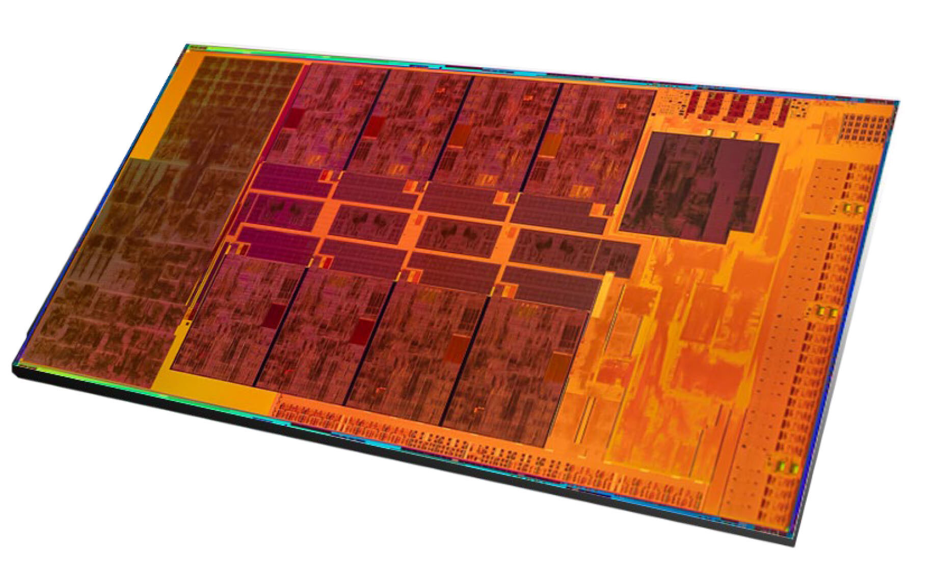
Intel is betting big on an 8-core processor to revive its gaming performance leadership, and that chip is the 11th Generation Core "Rocket Lake-S," coming this March. In its 2021 International CES online event, Intel disclosed more details about "Rocket Lake-S," including the first true-color die-shot. PC enthusiast @Locuza_ on Twitter annotated the die for your viewing pressure. For starters, nearly half the die-area of the "Rocket Lake-S" is taken up by the uncore and iGPU, with the rest going to the eight "Cypress Cove" CPU cores.
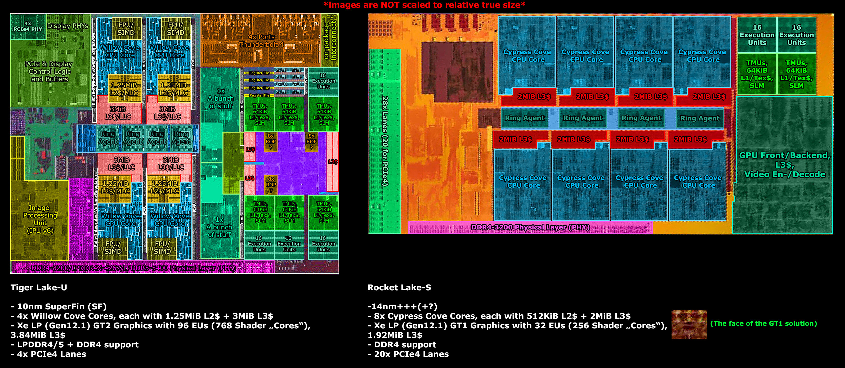
The "Cypress Cove" CPU core is reportedly a back-port of "Willow Cove" to the 14 nm silicon fabrication node, although there are some changes, beginning with its cache hierarchy. A "Cypress Cove" core is configured with the same L1I and L1D cache sizes as "Willow Cove," but differ with L2 and L3 cache sizes. Each "Cypress Cove" core is endowed with 512 KB of dedicated L2 cache (which is a 100% increase from the 256 KB on "Skylake" cores); but this pales in comparison to the 1.25 MB L2 caches of "Willow Cove" cores on the "Tiger Lake-U" silicon. Also, the L3 cache for the 8-core "Rocket Lake-S" die is 16 MB, spread across eight 2 MB slices; while the 4-core "Tiger Lake-U" features 12 MB of L3, spread across four 3 MB slices. Each core can address the whole L3 cache, across all slices.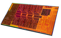
 The next big component on "Rocket Lake-S" is the Gen12 Xe-LP GT1 integrated graphics. The "GT1" differentiator denotes the smallest trim of Xe-LP, and amounts to 32 EU (execution units). The "Tiger Lake-U" silicon features the larger "GT2" trim of Gen12 Xe-LP, with 96 EU. Intel could give the GT1 on "Rocket Lake-S" some lavish clock boosting headroom on virtue of this being a desktop processor, to try and overcome some of the EU shortfall compared to "Tiger Lake-U." Even with just 32 EU, Intel is claiming a 50% iGPU performance gain compared to the Gen9.5 GT2 iGPU on "Comet Lake-S."
The third major component is the uncore, which looks visibly larger than the one on the 8-core "Coffee Lake Refresh" silicon. This is because it features a PCI-Express Gen 4.0 switching fabric, and additional SerDes to put out 28 PCIe lanes, compared to just 20 on the older generation. We imagine the memory controllers are largely unchanged, as Intel is sticking with dual-channel DDR4 as the memory standard for "Rocket Lake-S." The switch to DDR5 could probably herald a new socket, with "Alder Lake-S."
Sources:
Locuza_ (Twitter), PC Games Hardware
The "Cypress Cove" CPU core is reportedly a back-port of "Willow Cove" to the 14 nm silicon fabrication node, although there are some changes, beginning with its cache hierarchy. A "Cypress Cove" core is configured with the same L1I and L1D cache sizes as "Willow Cove," but differ with L2 and L3 cache sizes. Each "Cypress Cove" core is endowed with 512 KB of dedicated L2 cache (which is a 100% increase from the 256 KB on "Skylake" cores); but this pales in comparison to the 1.25 MB L2 caches of "Willow Cove" cores on the "Tiger Lake-U" silicon. Also, the L3 cache for the 8-core "Rocket Lake-S" die is 16 MB, spread across eight 2 MB slices; while the 4-core "Tiger Lake-U" features 12 MB of L3, spread across four 3 MB slices. Each core can address the whole L3 cache, across all slices.

The third major component is the uncore, which looks visibly larger than the one on the 8-core "Coffee Lake Refresh" silicon. This is because it features a PCI-Express Gen 4.0 switching fabric, and additional SerDes to put out 28 PCIe lanes, compared to just 20 on the older generation. We imagine the memory controllers are largely unchanged, as Intel is sticking with dual-channel DDR4 as the memory standard for "Rocket Lake-S." The switch to DDR5 could probably herald a new socket, with "Alder Lake-S."
17 Comments on Intel "Rocket Lake-S" Die Annotated
some may find die shots a private pleasure, while others prefers to dissect die-shots with an intense focus, a rush of blood as their eyes let our a laser-precision ray of concentration across the high definition image.
I also found 14nm+++(+?) very :roll:
It does still seem to have largely the same layout but there's like what... 10% reserved for the cores themselves?
Didn't they already figure out by now that approach is finite in terms of scaling? It echoes that they really don't, because they're still chasing 5 Ghz. What gives... are they too proud to copy chiplet designs or what?
Now, the real kicker for me, is why did they cut into cache size? If you need to cut somewhere, cut into the IGP. Hell, AMD has many (most?) of its desktop CPUs without an IGP at all and it's doing just fine.Even on the desktop you can see many tasks (mostly office related) don't actually scale that well with the number of cores*. And this is a mobile part.
AMD themselves have to resort to "what if you game while you stream at 4k" to make their CPUs look like they're using all those cores.
*You can still get good scaling up to 6 or 8 cores, but beyond that, it becomes very workload dependent.
It seems like the tiniest bit of reorganisation could have made a 48EU GT1 solution; For a start, QuickSync encode is a huge chunk of fixed-function hardware that is practically obsolete on higher-end desktop parts. Even though it's quick, it's miles behind even the old Pascal NVENC in speed and quality isn't great. If you're using QuickSync to shrink files you're in for a world of disappointment, because it's atrocious.
So yeah, QSV encode is increasingly niche, and honestly only seem to make sense for CPUs that go into NAS appliances, not desktop PCs. I'm pretty sure everyone cursing the pitiful 32EU IGP would much rather have had 50% or 100% more GPU horsepower....
In the real world, the game will run at whatever speed your GPU can spit out frames, but your encodes will run a little slower and your motherboard socket might turn into a puddle of hot slag under the 250W PL2 limit +/- whatever margin MSI and ASUS cheat by to try and gain an edge in benchmarks. I guess that's not really too different to the 10900K stunt processor/AKA space-heater.