News Posts matching #Gen12

Return to Keyword Browsing

Intel Xe iGPUs and Arc Graphics Lack DirectX 9 Support, Rely on API Translation to Play Older Games

So you thought your Arc A380 graphics card, or the Gen12 Xe iGPU in your 12th Gen Core processors were good enough to munch through your older games from the 2000s and early 2010s? Not so fast. Intel Graphics states that the Xe-LP and Xe-HPG graphics architectures, which power the Gen12 Iris Xe iGPUs and the new Arc "Alchemist" graphics cards, lack native support for the DirectX 9 graphics API. The two rely on API translation such as Microsoft D3D9On12, which attempts to translate D3D9 API commands to D3D12, which the drivers can recognize.

Older graphics architectures such as the Gen11 powering "Ice Lake," and Gen9.5 found in all "Skylake" derivatives, feature native support for DirectX 9, however when paired with Arc "Alchemist" graphics cards, the drivers are designed to engage D3D9On12 to accommodate the discrete GPU, unless the dGPU is disabled. API translation can be unreliable and buggy, and Intel points you to Microsoft and the game developers for support, Intel Graphics won't be providing any.

Intel's Day-0 Driver Updates Now Limited to Xe-based iGPUs and Graphics Cards

Intel Graphics, with its latest Graphics Drivers 31.0.101.3222, changed the coverage of its latest driver updates. The company would be providing game optimizations and regular driver updates only for its Gen12 (Iris Xe), and Arc "Alchemist" graphics products. Support for Gen9, Gen9.5, and Gen11 iGPUs integrated with 6th, 7th, 8th, 9th, and 10th generations of Intel processors, namely "Skylake," "Kaby Lake," "Coffee Lake," "Ice Lake," and "Cascade Lake," will be relegated to a separate, quarterly driver update cycle, which only covers critical updates and security vulnerabilities, but not game optimizations.

Intel's regular Graphics Driver cycle that includes Day-0 optimizations timed with new game releases, will only cover the Gen12 Xe iGPUs found in 11th Gen "Tiger Lake," "Rocket Lake," and 12th Gen "Alder Lake" processors; besides the DG1 Iris Xe graphics card; and Arc "Alchemist" discrete GPUs. Version 31.0.101.3222 appears to be a transitioning point, and so it has drivers from both branches included within a 1.1 GB package (the main branch supporting game optimizations for new GPUs, and the legacy branch for the older iGPUs). You can grab this driver from here.

Intel's Entry-level Core i3-12100 "Alder Lake" Beats Ryzen 3 3300X Comfortably

Intel's next entry-level processor for the Socket LGA1700 platform is the Core i3-12100. Carved out of the "Alder Lake-S" H0 silicon, this processor features 4 "Golden Cove" performance cores with HyperThreading enabling 8 logical processors, and no E-cores. The processor ticks at 3.30 GHz, with 4.30 GHz Turbo Boost 2.0 frequency. Each of the four cores has 1.25 MB of L2 cache, and they share 12 MB of L3 cache. The i3-12100 gets a Gen12 Xe LP-based iGPU, while a variant of the processor, the i3-12100F, lacks integrated graphics. Intel is rating the processor base power value at 60 W, with 77 W maximum turbo power.

XFastest scored an i3-12100 engineering sample, and wasted no time in comparing it with the Ryzen 3 3300X. The i3-12100 was tested on an ASRock Z690 Steel Legend motherboard that has DDR4 memory slots. 16 GB of dual-channel DDR4-3600 memory and RTX 3060 Ti were used on both the Intel and AMD test-beds. A Ryzen 3 3100 was also used on the AMD side. Right off the bat, we see the i3-12100 take a significant lead over the AMD chips at PCMark, posting a roughly 15% performance lead. Cinebench R23 is another test where the little "Alder Lake" scores big, posting a roughly 26% performance lead in the multi-threaded test, and 27% in the single-threaded test. This is mainly because the 3300X is based on "Zen 2" while the i3-12100 uses the cutting-edge "Golden Cove" cores. AMD hasn't bothered with "Zen 3" based Ryzen 3 desktop processors in the retail market.

Intel Announces 11th Gen Core "Tiger Lake-H" Mobile Processors

Intel today announced the 11th generation Core "Tiger Lake-H" mobile processors for notebooks of conventional thickness, gaming notebooks, and mobile workstations. This is the first scale-up of the "Tiger Lake" microarchitecture, with the introduction of a brand new die that has up to 8 "Willow Cove" CPU cores. These processors typically come with TDP of 35-45 W, but the flagship part ships with TDP as high as 65 W. Unlike "Rocket Lake," this chip is built on Intel's latest 10 nm SuperFin silicon fabrication process. With it, Intel is announcing ten processor SKUs—five each for the consumer and commercial notebook market segments. These span across the Core i9, Core i7, and Core i5 brand extensions.

The 10 nm "Tiger Lake-H" silicon measures roughly 190 mm², and has several changes compared to the 4-core "Tiger Lake-U" silicon the company debuted the 11th Gen with. The biggest change is the CPU core count of 8. This lets it not only achieve parity with AMD in mobile CPU core counts, but also purportedly beat it on the back of a higher IPC. Each of these 8 "Willow Cove" cores has 1.25 MB of dedicated L2 cache, and share 24 MB of L3 cache. You get the same "Willow Cove" ISA as the "Tiger Lake-U," including AVX-512 and DLBoost. Next up, the chip features an integrated graphics based on the Gen12 Xe LP graphics architecture, only that the execution units have reduced to just 32 on this silicon, compared to 96 on the 4-core Tiger Lake-U. The new chip enjoys a bigger power budget to run the iGPU at higher clock speeds. There is also a 20-lane PCI-Express Gen 4.0 interface, and a dual-channel DDR4 memory controller.

11th Gen Intel Core-H Specs Leaked: 8-core "Tiger Lake" a Reality

Intel's fabled 8-core "Tiger Lake-H" silicon built on the 10 nm SuperFin process, is close to reality. The company's upcoming 11th Gen Core "Tiger Lake-H" processors for performance- and gaming notebooks, leverages this die. An HD Tecnologia report leaks alleged company slides from Intel that detail the processor line up and feature-set. To begin with, the 11th Gen Core-H series processors come in core-counts ranging from 4-core/8-thread, to 6-core/12-thread, and 8-core/16-thread. Look at the embargo date on the leaked slides, one could expect a formal launch as close as May 11, 2021.

The 10 nm SuperFin "Tiger Lake-H" silicon features 8 "Willow Cove" CPU cores, and an updated iGPU based on the company's latest Gen12 Xe LP graphics architecture. Each of the eight CPU cores has 1.25 MB of L2 cache, and they share a massive 24 MB of L3 cache. The Gen12 Xe LP iGPU only has 32 execution units (EUs), according to the slides, 1/3rd those of the 96 EUs on the "Tiger Lake-U." The uncore component is also updated, now featuring dual-channel DDR4-3200 native support, and a 28-lane PCI-Express 4.0 root-complex. 16 of these lanes are wired out as PEG (PCI-Express Graphics), four as a CPU-attached NVMe slot, and eight toward the 8-lane DMI 3.0 chipset bus.

Intel Teases Xe HPG Gaming Graphics Architecture

Intel Graphics tweeted a marketing splash screen of its upcoming Xe HPG gaming discrete graphics architecture. There's not much to the video, except announcing the Xe HPG logo. It starts off with a depiction of the Xe LP architecture, on which the company's Gen12 iGPUs and Iris Xe MAX entry-level discrete GPUs are based; and swells into a larger silicon that grows in all directions. The animation could be a hint that Xe HPG chips will be an order of magnitude faster than the Iris Xe MAX, target serious gaming, and take the fight to both NVIDIA and AMD.

Intel is designing the Xe HPG graphics architecture for third-party silicon fabrication nodes, such as TSMC and Samsung, and could leverage a sub-10 nm node to significantly scale up from the Xe LP. A recent report pointed to the likelihood of 512 execution units on a certain Xe HPG variant (4,096 unified shaders) and contemporary GDDR6 memory, while Intel has the necessary IP to pull off DirectX 12 Ultimate logo readiness, including raytracing. Intel is likely eyeing a slice of the e-sports hardware segment, although a high-end GPU cannot be completely ruled out. Watch the video from the source link below.

Intel "Rocket Lake-S" Die Annotated

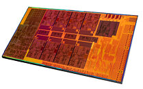
Intel is betting big on an 8-core processor to revive its gaming performance leadership, and that chip is the 11th Generation Core "Rocket Lake-S," coming this March. In its 2021 International CES online event, Intel disclosed more details about "Rocket Lake-S," including the first true-color die-shot. PC enthusiast @Locuza_ on Twitter annotated the die for your viewing pressure. For starters, nearly half the die-area of the "Rocket Lake-S" is taken up by the uncore and iGPU, with the rest going to the eight "Cypress Cove" CPU cores.

The "Cypress Cove" CPU core is reportedly a back-port of "Willow Cove" to the 14 nm silicon fabrication node, although there are some changes, beginning with its cache hierarchy. A "Cypress Cove" core is configured with the same L1I and L1D cache sizes as "Willow Cove," but differ with L2 and L3 cache sizes. Each "Cypress Cove" core is endowed with 512 KB of dedicated L2 cache (which is a 100% increase from the 256 KB on "Skylake" cores); but this pales in comparison to the 1.25 MB L2 caches of "Willow Cove" cores on the "Tiger Lake-U" silicon. Also, the L3 cache for the 8-core "Rocket Lake-S" die is 16 MB, spread across eight 2 MB slices; while the 4-core "Tiger Lake-U" features 12 MB of L3, spread across four 3 MB slices. Each core can address the whole L3 cache, across all slices.

8-core Intel "Tiger Lake-H" Processor by End of 2021

Intel at its recent 2021 International CES call confirmed the existence of an 8-core version of its 11th Gen Core "Tiger Lake" processor, and held the chip for the camera. The visibly bigger chip will be slated in Intel's H-segment (35 W to 45 W TDP), meaning it will only power gaming notebooks and mobile workstations; while the mainstream mobility segment will still be in the hands of its 4-core "Tiger Lake-H35" silicon. The 8-core "Tiger Lake-H" processor will also receive reasonably high clock-speeds, boosting up to 5.00 GHz.

Assuming the cache hierarchy and uncore/iGPU setup is unchanged between the 8-core and 4-core dies, we're looking at 24 MB of shared L3 cache, and 1.25 MB of dedicated L2 cache per core. These alone take up a big slice of the die-area. Add to this, the uncore features a PCI-Express Gen 4 root-complex and memory controllers that support dual-channel DDR4 and LPDDR4x memory types. The iGPU is expected to be based on the same Gen12 Xe-LP architecture as the 4-core die; although its execution unit count remains to be seen. In all likelihood, the 8-core "Tiger Lake-H" silicon is based on the same 10 nm SuperFin node.

Intel 11th Gen Core "Rocket Lake-S" Processor Detailed Some More

Intel at a January 11, 2021 online media event (which we live-blogged here) revealed more information about its 11th Generation Core "Rocket Lake-S" desktop processor family. These chips succeed the 10th Gen Core "Comet Lake-S," and are built on the same Socket LGA1200 package, retaining backwards compatibility with Intel 400-series chipset motherboards with firmware updates; and native support with the upcoming Intel 500-series chipset motherboards. Intel in its media event confirmed that the top Core i9-11900K is an 8-core/16-thread processor, which will deliver the highest PC gaming performance possible when it comes out.

In its media event, Intel revealed a side-by-side comparison of the i9-11900K with a machine powered by the AMD Ryzen 9 5900X 12-core processor, where it's shown offering a mostly mid-single-digit-percentage performance lead over the AMD chip. In the "Metro Exodus" benchmark prominently highlighted in the Intel event, the i9-11900K is shown offering an average frame-rate of 156.54 FPS compared to 147.43 FPS of the 5900X (a 6.17% gain). VideoCardz tweeted a leaked Intel presentation slide with many more game test results where Intel compared the two chips. Intel's play with marketing "Rocket Lake-S" to gamers and PC enthusiasts will hence ride on the back of gaming performance leadership, and future-proofing against the new wave of productivity apps that leverage AI deep-learning, as "Rocket Lake-S" features DLBoost VNNI extensions that accelerate deep-learning neural-net building, training, and AI inference performance.

Intel 11th Gen Core "Rocket Lake" Desktop TDP Values Surface

Intel's 11th Gen Core "Rocket Lake-S" desktop processors could feature similar TDP values to their 10th Gen "Comet Lake-S" predecessors, according to Momomo_us. Intel is preparing to give the Unlocked "K" and "KF" SKUs a TDP rating of 125 W, while the locked non-K models feature 65 W rating. The lineup is led by the 8-core/16-thread Core i9-11900K, followed by the locked i9-11900 and iGPU-devoid i9-11900F; the slightly slower 8-core/16-thread Core i7-11700K, followed by the i7-11700KF, i7-11700, and i7-11700F; and the 6-core/12-thread i5-10600K and its derivatives.

The 11th Gen Core desktop processor series arrives in Q1 2021, and is based on the 14 nm "Rocket Lake-S" silicon, and built into the Socket LGA1200 package, with backwards compatibility with Intel's 400-series chipset motherboards, and native support for the Intel 500-series. The "Rocket Lake-S" die is rumored to feature up to 8 "Cypress Cove" CPU cores, a dual-channel DDR4 memory controller, a 24-lane PCI-Express 4.0 root complex, and an updated Gen12 iGPU based on the Xe LP graphics architecture. The "Cypress Cove" CPU cores are reportedly 14 nm back-ports of the "Willow Cove" cores, and feature a double-digit percent IPC increase over the "Skylake" cores.

AMD RDNA2 Graphics Architecture Features AV1 Decode Hardware-Acceleration

AMD's RDNA2 graphics architecture features hardware-accelerated decoding of the AV1 video format, according to a Microsoft blog announcing the format's integration with Windows 10. The blog mentions the three latest graphics architectures among those that support accelerated decoding of the format—Intel Gen12 Iris Xe, NVIDIA RTX 30-series "Ampere," and AMD RX 6000-series "RDNA2." The AV1 format is being actively promoted by major hardware vendors to online streaming content providers, as it offers 50% better compression than the prevalent H.264 (translating into that much bandwidth savings), and 20% better compression than VP9. You don't need these GPUs to use AV1, anyone can use it with Windows 10 (version 1909 or later), by installing the AV1 Video Extension from the Microsoft Store. The codec will use software (CPU) decode in the absence of hardware acceleration.

Intel 11th Gen Core "Tiger Lake" & Xe Graphics Launch Event: Live Blog

Intel today launches its 11th Gen Core "Tiger Lake" mobile processors that introduce several new technologies on the backs of new IP. As described in the Architecture Day, "Tiger Lake" is built on the 10 nm SuperFin process, and combines new "Willow Cove" CPU cores with the first commercial debut of the Xe Gen12 graphics architecture that Intel is betting big on, to make a stab at the consumer graphics and scalar compute markets. Join us in this live-blog.

Update 16:00 UTC: GB (Gregory Bryant, EVP Client), leads the event from the comfort of his home.
Update 16:04 UTC: Here it is, the "world's best processor for thin and light laptops. You'll notice that like most Intel U-segment chips, this is an MCM of the processor and PCH die. Intel bases its "world's best" claims on a per-segment basis.

Intel 11th Gen Core "Tiger Lake" Promotional Videos Leak

Promotional videos of Intel 11th Gen Core "Tiger Lake" processors leaked to the web courtesy h0x0d on Twitter. It confirms the new corporate identity of Intel, along with its new logo artistic language. It also confirms the new EVO Powered by Core brand extension, along with a separate case badge for notebooks that use Iris Xe discrete graphics (DG1) in addition to the Xe Gen12 iGPU of "Tiger Lake." Intel has a technology that can get the Xe LP iGPU and dGPU to work in tandem. VideoCardz compiled some interesting frames from the promotional videos, revealing bits such as clock speeds of up to 4.80 GHz (boost), 3.11 GHz (base), the first "Tiger Lake" parts being 4-core/8-thread, the new 10 nm SuperFin transistor, wafer- and die shots of "Tiger Lake" 4c+96EU die, and unless we're mistaken, pictures of a "Tiger Lake" package that uses a DRAM (HBM?) stack on-package, using EMIB. h0x0d also posted videos of the Lenovo Yoga 9i and HP Spectre notebooks based on "Tiger Lake."

Intel "Willow Cove" Core, Xe LP iGPU, and "Tiger Lake" SoC Detailed

A lot is riding for Intel on its 11th Gen Core "Tiger Lake" system-on-chip (SoC), which will launch exclusively on mobile platforms, hoping to dominate the 7 W thru 15 W ultraportable form-factors in 2020, while eventually scaling up to the 25 W thru 45 W H-segment form-factors in 2021, with a variant that is rumored to double core-counts. The chip is built on Intel's new 10 nm SuperFin silicon fabrication node that enables a double digit percentage energy efficiency growth over 10 nm, allowing Intel to significantly dial up clock speeds without impacting the power envelope. The CPU and iGPU make up the two key components of the "Tiger Lake" SoC.

The CPU component on the "Tiger Lake" processors that launch in a few weeks from now features four "Willow Cove" CPU cores. Coupled with HyperThreading, this ends up being a 4-core/8-thread setup, although much of Intel's innovation is in giving these cores significant IPC increases over the "Skylake" core powering "Comet Lake" processors, and compared to the "Sunny Cove" cores powering "Ice Lake" a minor IPC (although major net performance increase from clock speeds). The "Willow Cove" CPU core appears to be a derivative of the "Sunny Cove" core, designed to take advantage of the 10 nm SuperFin node, along with three key innovations.

Coreboot Code Hints at Intel "Alder Lake" Core Configurations

Intel's 12th Gen Core EVO "Alder Lake" processors in the LGA1700 package could introduce the company's hybrid core technology to the desktop platform. Coreboot code leaked to the web by Coelacanth's Dream sheds fascinating insights to the way Intel is segmenting these chips. The 10 nm chip will see Intel combine high-performance "Golden Cove" CPU cores with energy-efficient "Gracemont" CPU cores, and up to three tiers of the company's Gen12 Xe integrated graphics. The "Alder Lake" desktop processor has up to eight big cores, up to eight small ones, and up to three tiers of the iGPU (GT0 being disabled iGPU, GT1 being the lower tier, and GT2 being the higher tier).

Segmentation between the various brand extensions appears to be primarily determined by the number of big cores. The topmost SKU has all 8 big and 8 small cores enabled, along with GT1 (lower) tier of the iGPU (possibly to free up power headroom for those many cores). The slightly lower SKU has 8 big cores, 6 small cores, and GT1 graphics. Next up, is 8 big cores, 4 small cores, and GT1 graphics. Then 8+2+GT1, and lastly, 8+0+GT1. The next brand extension is based around 6 big cores, being led by 6+8+GT2, and progressively lower number of small cores and their various iGPU tiers. The lower brand extension is based around 4 big cores with similar segmentation of small cores, and the entry-level parts have 2 big cores, and up to 8 small cores.

AMD Ryzen 7 4700G "Renoir" iGPU Showing Playing Doom Eternal 1080p by Itself

Hot on the heels of a June story of a 11th Gen Core "Tiger Lake" processor's Gen12 Xe iGPU playing "Battlefield V" by itself (without a graphics card), Tech Epiphany bring us an equally delicious video of an AMD Ryzen 7 4700G desktop processor's Radeon Vega 8 iGPU running "Doom Eternal" by itself. id Software's latest entry to the iconic franchise is well optimized for the PC platform to begin with, but it's impressive to see the Vega 8 munch through this game at 1080p (1920 x 1080 pixels) no resolution scaling, with mostly "High" details. The game is shown running at frame-rates ranging between 42 to 47 FPS, with over 37 FPS in close-quarters combat (where the enemy models are rendered with more detail).

With 70% resolution scale, frame rates are shown climbing 50 FPS. At this point, when the detail preset is lowered to "Medium," the game inches close to the 60 FPS magic figure, swinging between 55 to 65 FPS. The game is also shown utilizing all 16 logical processors of this 8-core/16-thread processor. Despite just 8 "Vega" compute units, amounting to 512 stream processors, the iGPU in the 4700G has freedom to dial up engine clocks (GPU clocks) all the way up to 2.10 GHz, which helps it overcome much of the performance deficit compared to the Vega 11 solution found with the previous generation "Picasso" silicon. Watch the Tech Epiphany video presentation in the source link below.

Intel to Detail Xe Graphics on August 13

Intel is expected to reveal technical details of its upcoming Xe graphics architecture on August 13, according to a tweet by Intel Graphics that has since been deleted. Tom's Hardware believes the reveal is still on the cards. "You've waited. You've wondered. We'll deliver. In 20 days, expect more details on Xe graphics," the tweet read. Senior Fellow and Director of Graphics Architecture at Intel, David Blythe is expected to present a technical brief on the Xe graphics architecture at a Hot Chips 2020 virtual event on August 17.

These technical reveals are closely timed with the launch of "Tiger Lake," Intel's first commercial debut of Xe as an iGPU solution the chipmaker refers to as "Gen12" for consistency with older generations of integrated graphics. Xe is far from designed for just iGPU or small dGPUs, with the architecture being scalable all the way up to large scalar compute processors the size of beer mug coasters. Even as an iGPU, Xe is formidable, as it was recently shown playing AAA games by itself. Recent commentary from Intel at its Q2 2020 financial results provided strong hints of Xe dGPUs being de-coupled from Intel's foundry woes, and possibly headed for third-party foundries such as Samsung or TSMC.

Intel Linux Patch Confirms "Alder Lake" is a Hybrid Core Processor

A Linux kernel patch contributed and signed off by Intel confirms that its upcoming Core "Alder Lake" processor will feature a hybrid core topology, much like Core Hybrid "Lakefield." The patch references "Lakefield" and "Alder Lake" under "Hybrid Core/Atom Processors." The patch possibly gives the Linux kernel awareness of the hybrid core topology, so it can schedule its work between the two types of cores on the silicon accordingly, and avoid rotating between the two core groups. Under the Android project, Linux has been aware of a similar tech from Arm since 2013.

Analogous with Arm big.LITTLE, the Intel Hybrid Core technology involves two kinds of CPU cores on a processor die, the first kind being "high performance," and the second being "low power." On "Lakefield," Intel deployed one "Sunny Cove" high performance core, and four "Tremont" low power cores. The low power cores keep the machine ticking through the vast majority of time when processing workloads requiring the high performance cores aren't present. With "Alder Lake," Intel is expected to scale up this concept, with the silicon rumored to feature eight "Golden Cove" high performance cores, and eight "Gracemont" low power ones. The chip is also expected to feature a Gen12 Xe iGPU.

Intel Gen12 iGPU on "Rocket Lake" will be Slimmer than the one on "Tiger Lake"?

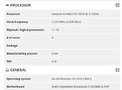
The Gen12 Xe integrated graphics component of the upcoming "Rocket Lake-S" desktop processor will be slimmer than the one on the upcoming 10 nm "Tiger Lake" silicon, according to a Geekbench hardware detection unearthed by TUM_APISAK. An 8-core/16-thread "Rocket Lake-S" sample surfaced on the Geekbench database, which shows the iGPU to feature 32 compute units as read by the OpenCL benchmark (corresponding with 32 execution units), compared to 96 on the "Tiger Lake-U" mobile processor die. The iGPU is also clocked rather conservatively on this ES, at at 1.15 GHz. The CPU component, on the other hand, ticks at 3.20 GHz, boosting up to 4.30 GHz. It's likely that with the power budget of the desktop platform, the iGPU will be able to sustain boost frequencies better.

Intel "Tiger Lake" Gen12 Xe iGPU Shown Playing "Battlefield V" By Itself

In what is possibly the first taste of Intel's Gen12 Xe iGPU running a AAA game, Ryan Shrout, chief performance strategist at Intel, showed off a prototype notebook running a "Tiger Lake" processor that is playing "Battlefield V" by itself (without discrete graphics). "Perks of the job! Took a prototype Tiger Lake system for a spin on Battlefield V to stretch its legs. Impressive thin and light gaming perf with Xe graphics! Early drivers/sw, but it's the first time I've seen this game run like this on integrated gfx. More later this year!," said Shrout.

The gameplay video (linked as source below), shows a playable experience for "Battlefield V" with Gen12 Xe, with 1080p at around 30 Hz. It only serves to appetize us for what would come next, when Intel scales up this IP to discrete GPUs. The Gen12 Xe iGPU appears capable of e-sports gaming with the right settings, and could spell serious trouble for cheap dGPU solutions such as the GeForce MX series or Radeon RX 530 series.

Intel "Rocket Lake-S" a Multi-Chip Module of 14nm Core and 10nm Uncore Dies?

VLSI engineer and industry analyst, @chiakokhua, who goes by "Retired Engineer" on Twitter, was among the very first voices that spoke about 3rd gen Ryzen socket AM4 processors being multi-chip modules of core- and uncore dies built on different silicon fabrication processes, which was an unbelievable theory at the time. He now has a fantastic theory of what "Rocket Lake-S" could look like, dating back to November 2019, which is now re-surfacing on tech communities. Apparently, Intel is designing these socket LGA1200 processors to be multi-chip modules, similar to "Matisse" in some ways, but different in others.

Apparently, "Rocket Lake-S" is a multi-chip module of a 14 nm die that holds the CPU cores; and 10 nm die that holds the uncore components. AMD "Matisse" and "Vermeer" too have such a division of labor, but the CPU cores are located on dies with a more advanced silicon fabrication process (7 nm), than the die with the uncore components (12 nm).

Intel "Tiger Lake" Gen12 Xe iGPU Compared with AMD "Renoir" Vega 8 in 3DMark "Night Raid"

Last week, reports of Intel's Gen12 Xe integrated graphics solution catching up with AMD's Radeon Vega 8 iGPU found in its latest Ryzen 4000U processors in higher-tier 3DMark tests sparked quite some intrigue. AMD's higher CPU core-count bailed the processor out in overall 3DMark 11 scores. Thanks to Thai PC enthusiast TUM_APISAK, we now have a face-off between the Core i7-1165G7 "Tiger Lake-U" processor (15 W), against AMD Ryzen 7 4800U (15 W), and the mainstream-segment Ryzen 7 4800HS (35 W), in 3DMark "Night Raid."

The "Night Raid" test is designed to evaluate iGPU performance, and takes advantage of DirectX 12. The Core i7-1165G7 falls behind both the Ryzen 7 4800U and the 4800HS in CPU score, owing to its lower CPU core count, despite higher IPC. The i7-1165G7 is a 4-core/8-thread chip featuring "Willow Cove" CPU cores, facing off against 8-core/16-thread "Zen 2" CPU setups on the two Ryzens. Things get interesting with graphics tests, where the Radeon Vega 8 solution aboard the 4800U scores 64.63 FPS in GT1, and 89.41 FPS in GT2; compared to just 27.79 FPS in GT1 and 32.05 FPS in GT2, by the Gen12 Xe iGPU in the i7-1165G7.

Intel "Tiger Lake" vs. AMD "Renoir" a Pitched Battle on 3DMark Database

Intel's 11th generation Core i7-1165G7 "Tiger Lake-U" processor armed with 4 "Willow Cove" cores and Gen12 Xe graphics fights a pitched battle against AMD Ryzen 7 4800U "Renoir" (8 "Zen 2" cores and Radeon Vega 8 graphics), courtesy of some digging by Thai PC enthusiast TUM_APISAK. The 4800U beats the i7-1165G7 by a wafer-thin margin of 1.9% despite double the CPU core-count and a supposedly advanced iGPU, with 6331 points as against 6211 points of the Intel chip, in 3DMark 11. A breakdown of the score reveals fascinating details of the battle.

The Core i7-1165G7 beats the Ryzen 7 4800U in graphics tests, with a graphics score of 6218 points, against 6104 points of the 4800U, resulting in a 1.9% lead. In graphics tests 1, 2, and 3, the Gen12 Xe iGPU is 7.3-8.9% faster than the Radeon Vega 8, through translating to 2-4 FPS. The Intel iGPU crosses the 30 FPS mark in these three tests. With graphics test 4, the AMD iGPU ends up 8.8% faster. Much of AMD's performance gains come from its massive 55.6% physics score lead thanks to its 8-core/16-thread CPU, which ends up beating the 4-core/8-thread "Willow Cove," with the 4800U scoring 12494 points compared to 8028 points for the i7-1165G7. This CPU muscle also plays a big role in graphics test 4. This battle provides sufficient basis to speculate that "Tiger Lake-U" will have a very uphill task matching "Renoir-U" chips such as the Ryzen 7 4800U, and the upcoming Ryzen 9 4900U (designed to compete with the i7-1185G7).

No Intel "Rocket Lake-S" or "Ice Lake-X" This Year?

A roadmap slide from an Intel Partner Connect presentation suggests that the company's client-segment processor lineup will be unchanged for the rest of 2020, with the company briskly launching its 10th generation "Comet Lake-S" desktop processor lineup through May-June, and "Comet Lake-H" a month prior. The Core X "Cascade Lake-X" processor lineup will continue to lead the company in the high core-count HEDT segment, with no indications of new models, at least none higher than 18 cores.

More importantly, this slide dulls expectations of the company refreshing its desktop process segment just before Holiday 2020 with the 11th generation "Rocket Lake-S" silicon that has next-gen "Willow Cove" CPU cores, Gen12 Xe integrated graphics, and PCIe gen 4.0 connectivity, especially with engineering samples of the chips already hitting the radar. Intel is expected to launch 10 nm "Ice Lake-SP" Xeon enterprise processors in 2020, and there was hope for some of this IP to power Intel's next HEDT platform, the fabled "Ice Lake-X," especially with AMD's "Castle Peak" 3rd gen Threadrippers dominating this segment. While there's little doubt that the slide may have originated from Intel, its context must be studied. Partner Connect is a platform for Intel to interact with its channel partners (distributors, retailers, system integrators, etc), and information about future products is far more restricted on these slides, than presentations intended for large OEMs, motherboard manufacturers, etc. Then again, with the COVID-19 pandemic throwing supply chains off rails, it wouldn't surprise us if this slide spells Gospel.

Intel 8-core/16-thread "Rocket Lake-S" Processor Engineering Sample 3DMarked

The "Rocket Lake-S" microarchitecture by Intel sees the company back-port its next-generation "Willow Cove" CPU core to the existing 14 nm++ silicon fabrication process in the form of an 8-core die with a Gen12 Xe iGPU. An engineering sample of one such processor made it to the Futuremark database. Clocked at 3.20 GHz with 4.30 GHz boost frequency, the "Rocket Lake-S" ES was put through 3DMark "Fire Strike" and "Time Spy," with its iGPU in play, instead of a discrete graphics card.

In "Fire Strike," the "Rocket Lake-S" ES scores 18898 points in the physics test, 1895 points in the graphics tests, and an overall score of 1746 points. With "Time Spy," the overall score is 605, with a CPU score of 4963 points, and graphics score of 524. The 11th generation Core "Rocket Lake-S" processor is expected to be compatible with existing Intel 400-series chipset motherboards, and feature a PCI-Express gen 4.0 root complex. Several 400-series chipset motherboards have PCIe gen 4.0 preparation for exactly this. The increased IPC from the "Willow Cove" cores is expected to make the 8-core "Rocket Lake-S" a powerful option for gaming and productivity tasks that don't scale across too many cores.
Return to Keyword Browsing
May 21st, 2024 11:31 EDT change timezone

New Forum Posts

Popular Reviews

Controversial News Posts