Tuesday, July 27th 2021

Intel Rebadges 10nm Enhanced SuperFin Node as "Intel 7," Invents Other Creative Node Names
Intel, in a move comparable to its competitors' Performance Rating system from the 1990s, has invented a new naming scheme for its in-house foundry nodes to claim technological parity with contemporaries such as TSMC and Samsung, that are well into the sub-10 nm class. Back in the i586 era, when Intel's competitors such as AMD and Cyrix, couldn't keep up with its clock-speeds yet found their chips to be somewhat competitive, they invented the PR (processor rating) system, with a logical number attempting to denote parity with an Intel processor's clock-speed. For example, a PR400 processor rating meant that the chip rivaled a Pentium II 400 MHz (which it mostly didn't). The last that the PR system made sense was with the final generation of single-core performance chips, Pentium 4 and Athlon XP, beyond which, the introduction of multi-core obfuscated the PR system. A Phenom X4 9600 processor didn't mean performance on par with a rival Intel chip running at an impossible 9.60 GHz.
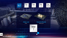
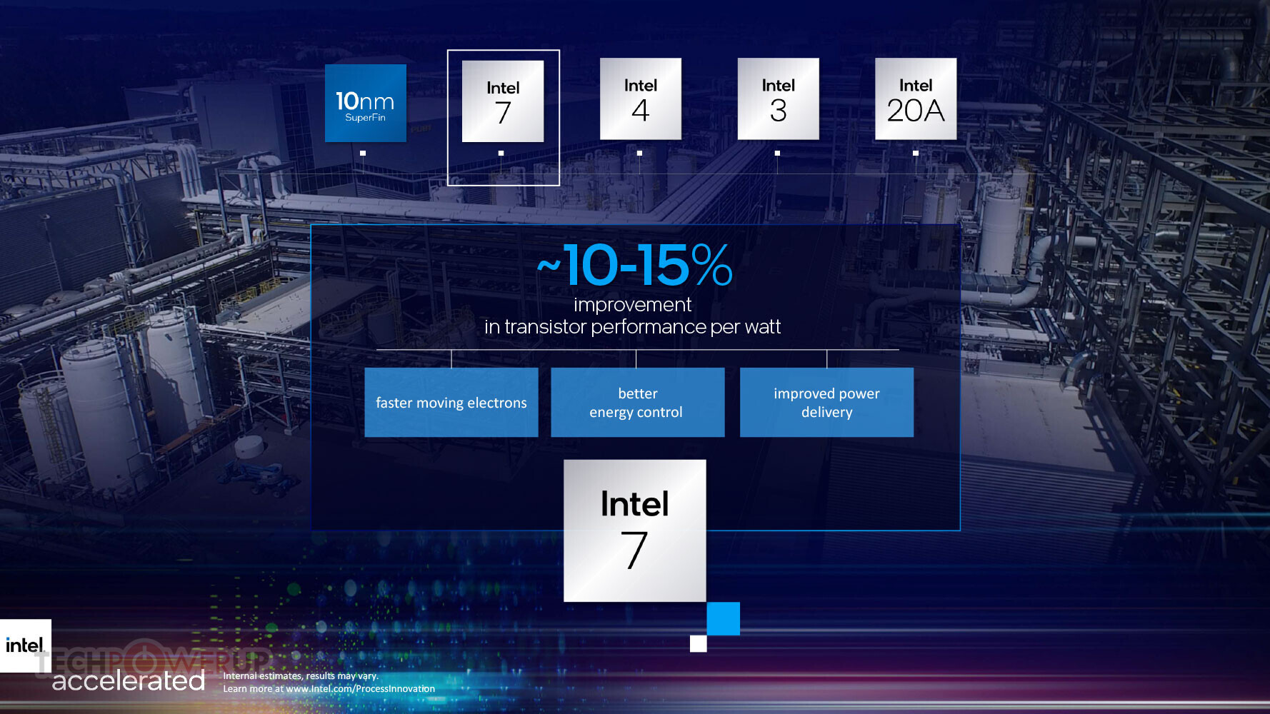
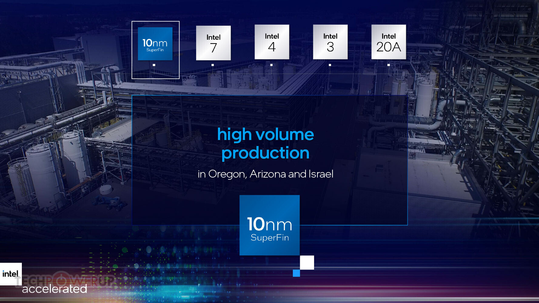
Intel's new foundry naming system sees its 10 nm Enhanced SuperFin node re-badge as "Intel 7." The company currently builds 11th Gen Core "Tiger Lake" processors on the 10 nm SuperFin node, and is expected to build its upcoming 12th Gen Core "Alder Lake" chips on its refinement, the 10 nm Enhanced SuperFin, which will now be referred to as "Intel 7." The company is careful to avoid using the nanometer unit next to the number, instead signaling the consumer that the node somehow offers transistor density and power characteristics comparable to a 7 nm node. Intel 7 offers a 10-15 percent performance/Watt gain over 10 nm SuperFin, and is already in volume production, with a debut within 2021 with "Alder Lake."

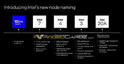

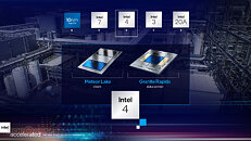

 This is where things get interesting. The successor to Intel 7 is named Intel 4, and is technically a 7 nm EUV node. This node offers a 20 percent performance/Watt gain over Intel 7 (aka 10 nm Enhanced SuperFin), and will debut in mid-2022 with "Meteor Lake" client- and "Granite Rapids" enterprise processors. Intel has gone with "4" for the name as 2022 sees both Samsung and TSMC roll out their sub-5 nm nodes. TSMC will debut the 4 nm, while Samsung will hopefully iron out its 5 nm yield issues, and ramp up 4 nm, by 2022.
 Intel 3 succeeds Intel 4 in the second half of 2023, and is timed to launch around the time TSMC comes out with its sub-4 nm node, likely the 2 nm. Intel claims this node offers an 18 percent performance/Watt gain over the Intel 4, implement a denser HP library, increase the use of EUV, improve the drive-current and via resistance, to result in the performance/Watt target. With no mention of FET size, it's very likely that Intel 3 is still a 7 nm node.


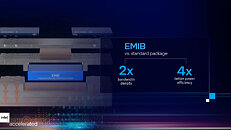
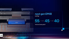
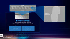
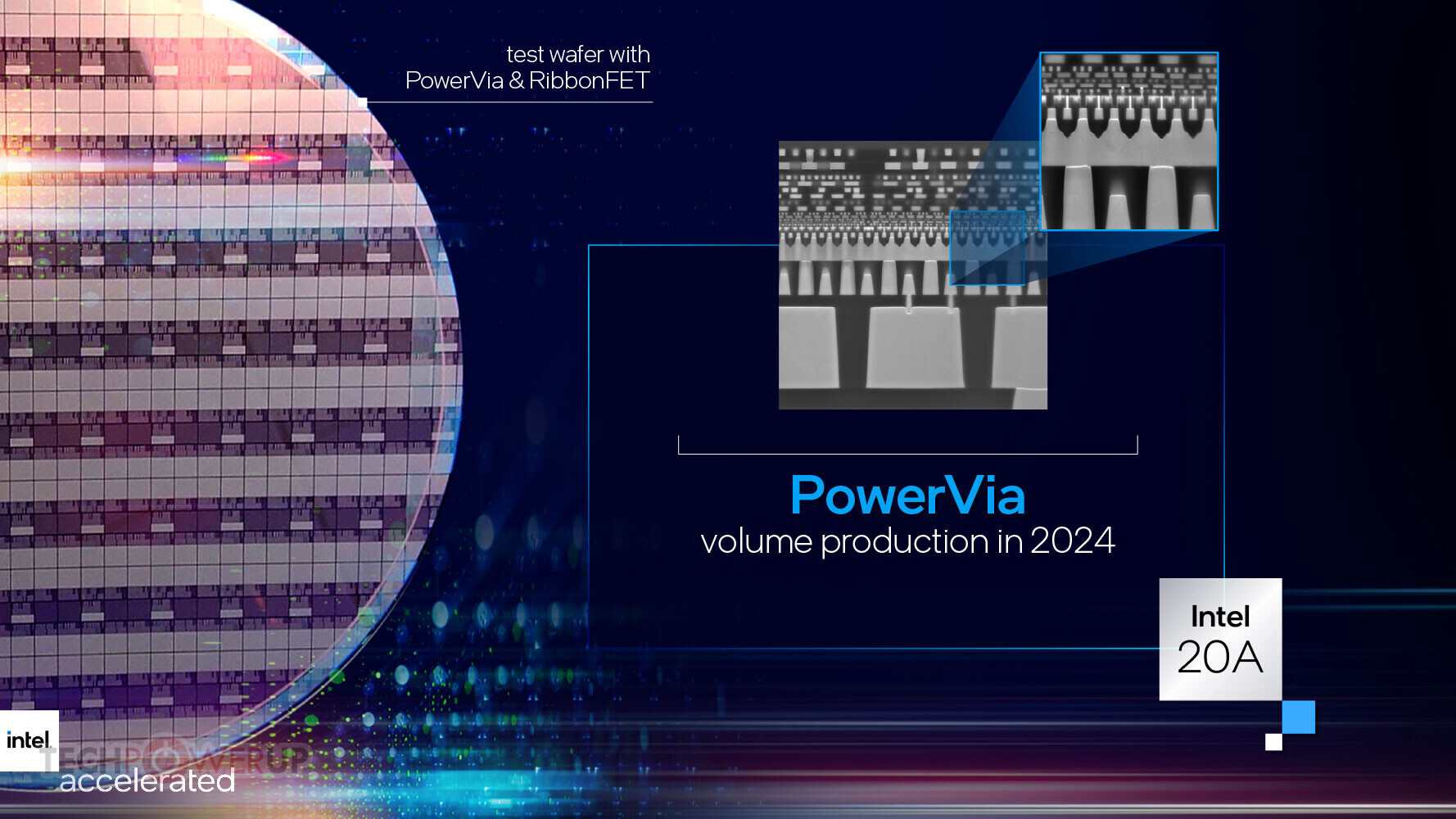
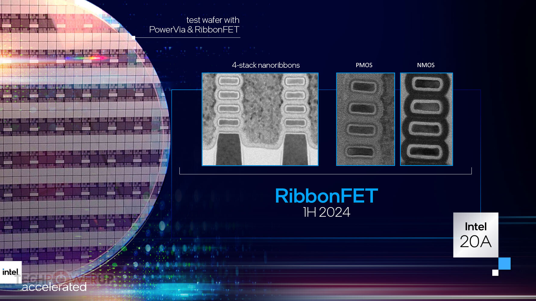
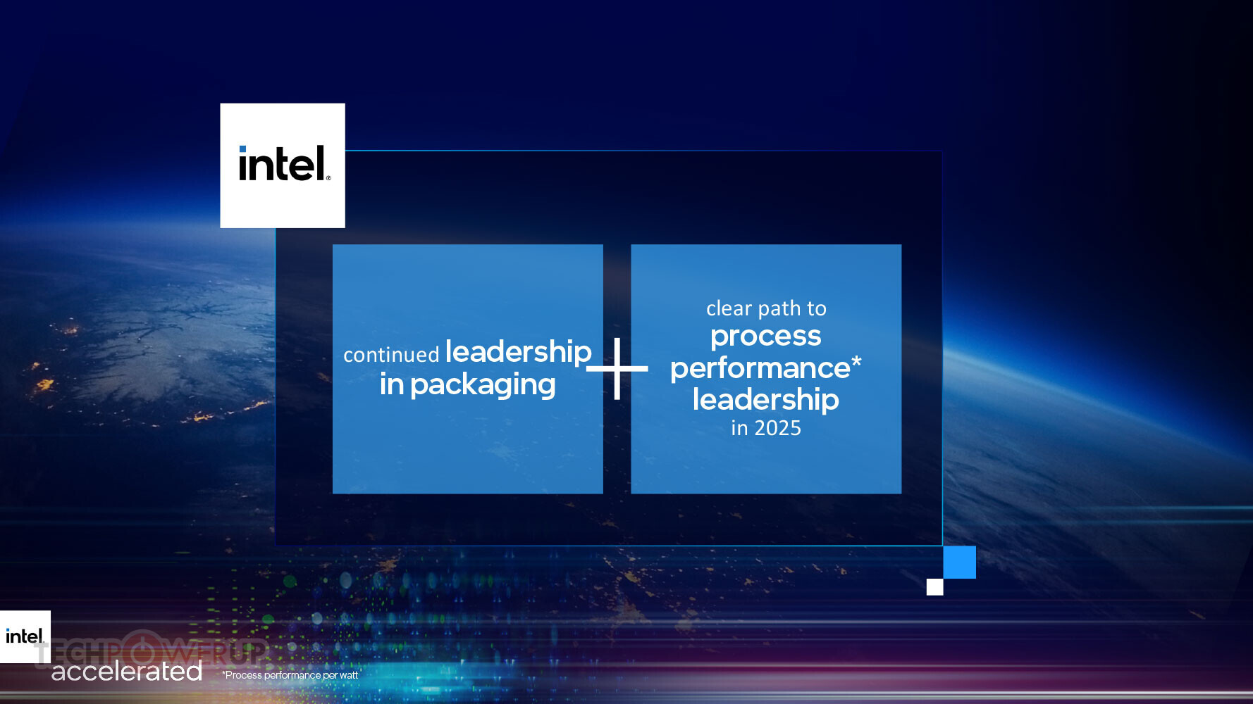
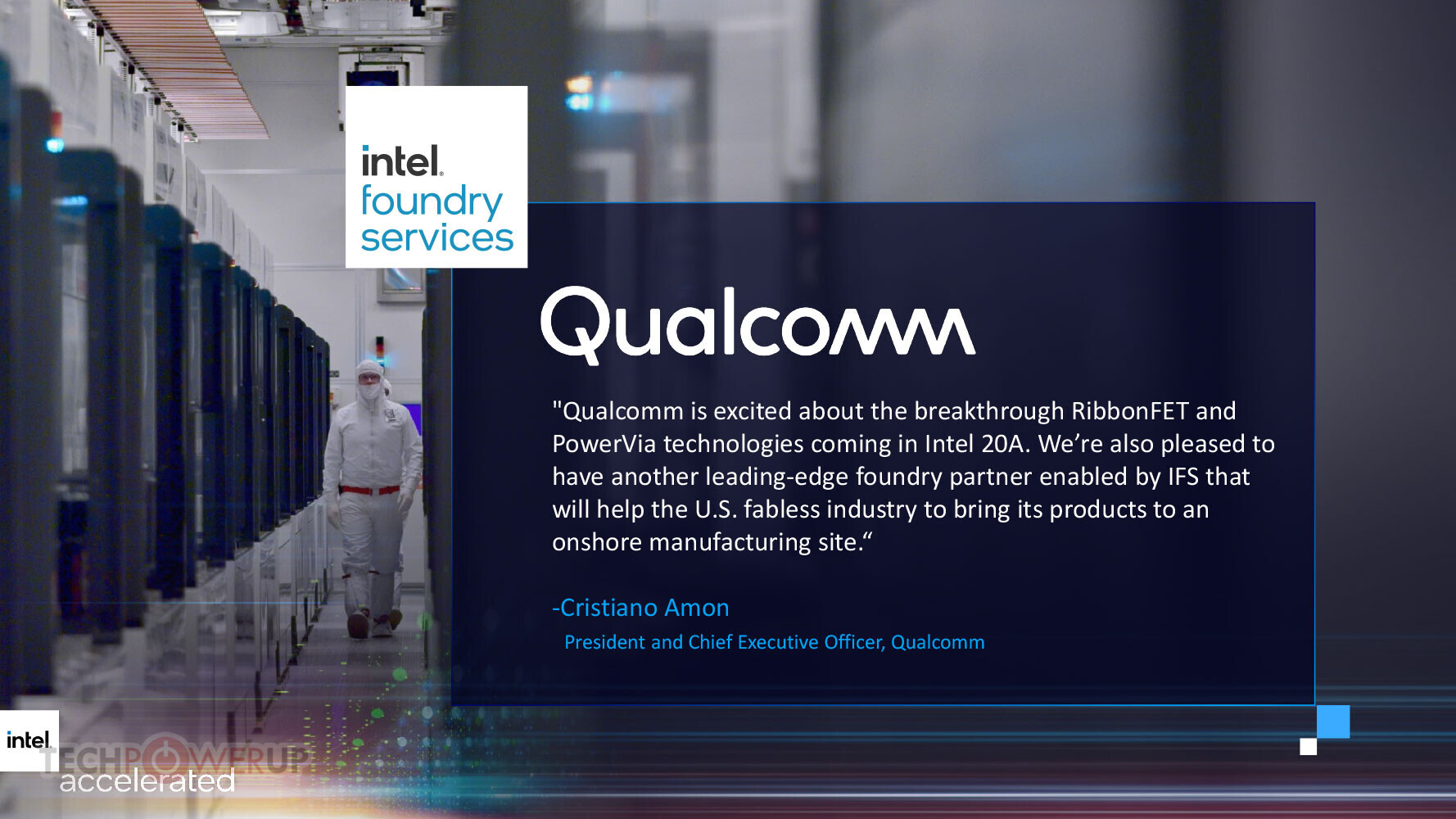
 It's only in 2024 that Intel is promising major technological breakthroughs, with Intel 20A, heralding the era in silicon fabrication where transistor sizes are measured in Angstroms (0.1 nm). 20A would hence be a creative way of saying 2 nm. Intel will introduce a brand new transistor design it calls the RibbonFET. It remains to be seen if this is a whole new innovation or similar to nanosheet FETs. Intel is also announcing PowerVia, a revolutionary new way to connect silicon dies with each other, or with the package, which debuts with the Intel 20A node. The company is targeting a 1H-2024 debut of this new node.
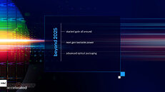
With these, Intel is ensuring that it has a new node to offer each year leading up to 2024, each with a double-digit percent performance/Watt gain, so the company can restore something resembling its "Tick-Tock" product development cadence, enabling it to compete not just against AMD, but also the emergence of serious Arm-powered rivals, such as NVIDIA, Qualcomm, and Apple. The company is hence facing similar levels of competition as the early 1990s. x86 may no longer have a stranglehold over the PC, as Arm-powered rivals claw away at market-share with efficient and fairly-powerful chips.
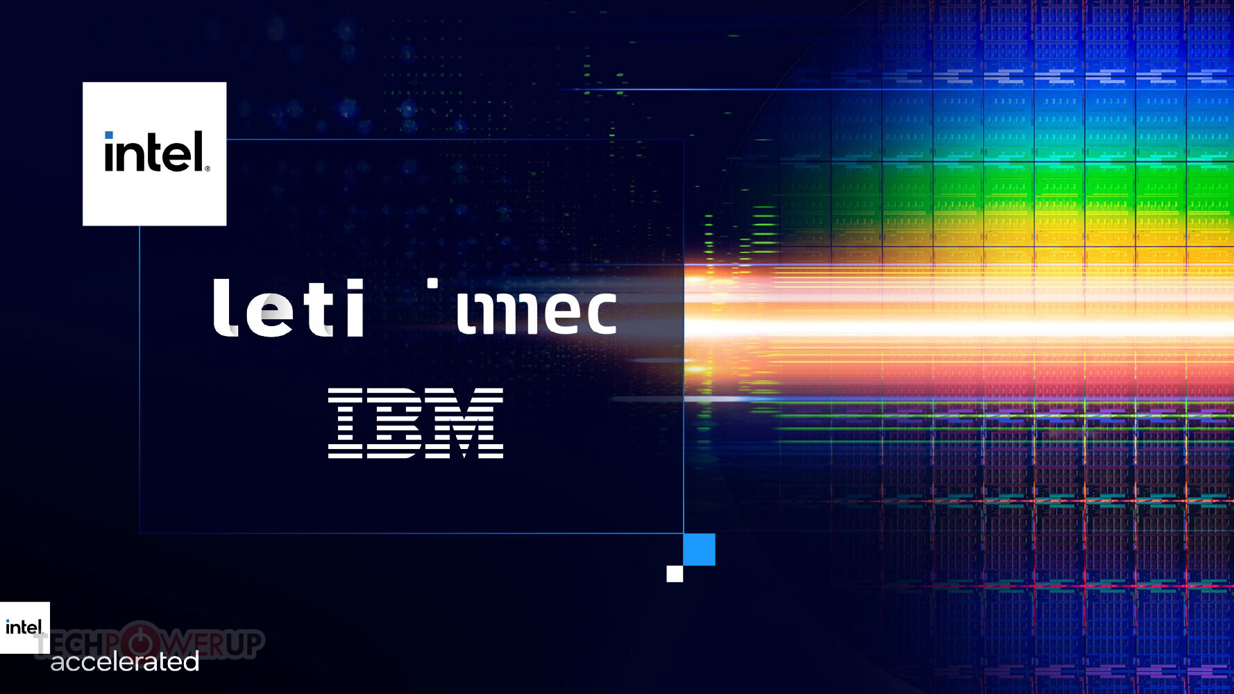
The complete slide-deck follows.


Source:
VideoCardz
Intel's new foundry naming system sees its 10 nm Enhanced SuperFin node re-badge as "Intel 7." The company currently builds 11th Gen Core "Tiger Lake" processors on the 10 nm SuperFin node, and is expected to build its upcoming 12th Gen Core "Alder Lake" chips on its refinement, the 10 nm Enhanced SuperFin, which will now be referred to as "Intel 7." The company is careful to avoid using the nanometer unit next to the number, instead signaling the consumer that the node somehow offers transistor density and power characteristics comparable to a 7 nm node. Intel 7 offers a 10-15 percent performance/Watt gain over 10 nm SuperFin, and is already in volume production, with a debut within 2021 with "Alder Lake."


With these, Intel is ensuring that it has a new node to offer each year leading up to 2024, each with a double-digit percent performance/Watt gain, so the company can restore something resembling its "Tick-Tock" product development cadence, enabling it to compete not just against AMD, but also the emergence of serious Arm-powered rivals, such as NVIDIA, Qualcomm, and Apple. The company is hence facing similar levels of competition as the early 1990s. x86 may no longer have a stranglehold over the PC, as Arm-powered rivals claw away at market-share with efficient and fairly-powerful chips.
The complete slide-deck follows.


101 Comments on Intel Rebadges 10nm Enhanced SuperFin Node as "Intel 7," Invents Other Creative Node Names
At best, we can compare transistor density. That's about it since rarely if ever any design is ported to multiple foundries' nodes
No one's doubting that TSMC and Samsung love to give old shit a new coat of paint and call it by a new name, but when you can't even deliver compelling products, it doesn't matter if your node is denser or more efficient than the name suggests or that the competitors are misleading consumers. 10SF is much improved and dense as hell - so what? Tiger Lake is still a power hog and ICL Xeon isn't impressive.
At least begin the new naming scheme on the (former) 7nm node. A fresh start to forget about the 10nm debacle, if you will - I thought that was exactly what Pat aimed for when he became CEO? I get that they want to pull out all the stops for Alder Lake and Sapphire Rapids, but shit like this just reeks of a lack of confidence in Alder Lake.
That said, the news post in certain parts reads like a highly suspect opinion piece rather than news.
Im suprised they actually went past 10 with the processor names, personally I dont have a problem with 12900k but I guess a lot of people do because usually that is the moment to start over.
I guess Intel are really feeling the heat these days ! They have been talking it up big time how good their future products will be! What about their current products ! Then having to rename their products to show how they compare to their competitors, must be a first for Intel ! Normally they just make the product and everyone else has to follow! Intel having to drop the price on their processors, must be a first !
I have to say i get sick of hearing about Intel this and that but at the end of the day whether their 10nm is better than TSMC 7nm etc or not show us some products! TSMC make products!
All good to sprout about it with nothing to show for it!
and heck, even if the numbers were a representation of reality, who cares?
If Intel would make a chip on 4nm whereas AMD would be 7nm but the AMD chip consumes less power and is faster, then who cares that the Intel one would be build on a smaller node? nobody.
We associate a lower nm number with performance but ultimately we only care about that performance soooo....yeah who cares, just wait for reviews on the actual product.
although i am sure it will be misleading in some ways ... some will think "Intel is definitely better in all aspect since their bigger node are same as AMDs smaller node" and not look at the real result ... just like the 12900K beating a 5950X (kinda a pointless PR move ... next gen beating previous gen ... even tho it shows the good point of big core small core nonetheless)
the pricing and availability will always dictate for me ... not the PR
if it was like that i would have taken a 11600K to replace my 6600K and not a R5 3600 which albeit being previous gen still hold up to the 11600K (no... i do not consider a few fps more to be an abyssal gape or a "Intel destroy AMD in gaming!" validation )
i mean it like "IN ALL ASPECT" ... which in reality it is not the case... beating in PR slides is one thing... optimized and standardized "variable" do wonder... sure the 12900k beat a 5950X now ... but what would it be actually with the correct counterpart in a benchmark from a trusted reviewer and not just some PR without context and background. (it's Intel we are talking ... and "i disliked Intel behavior these last years" is a reflection on how low they dived once they got their challenge met with Ryzen)
edit: also yes the bigger node packing more transistor is bound to be better than a smaller node with less transistor ... ;)
There's no doubt Intel was sore at losing their crown. Love em or hate em though, i have no doubt they will be back.
Whether Intel wants to or not (while the obviously do want) they need to use the process improvements for marketing as long as AMD piggybacks on TSMCs marketing for the same.
Intel 14nm transistor size (as measured by crazy German dude):
24 by 24 nm
TSMC 7nm
22 by 22 nm
not talkignore the rest of Intel about what they are planning on doing.Its all just rumours and leaked preproduction parts ! Take it all with a grain of salt !
I am half expecting the empire to strike back but its looking likely to be a few years away just yet!