News Posts matching #Intel 3

Return to Keyword Browsing

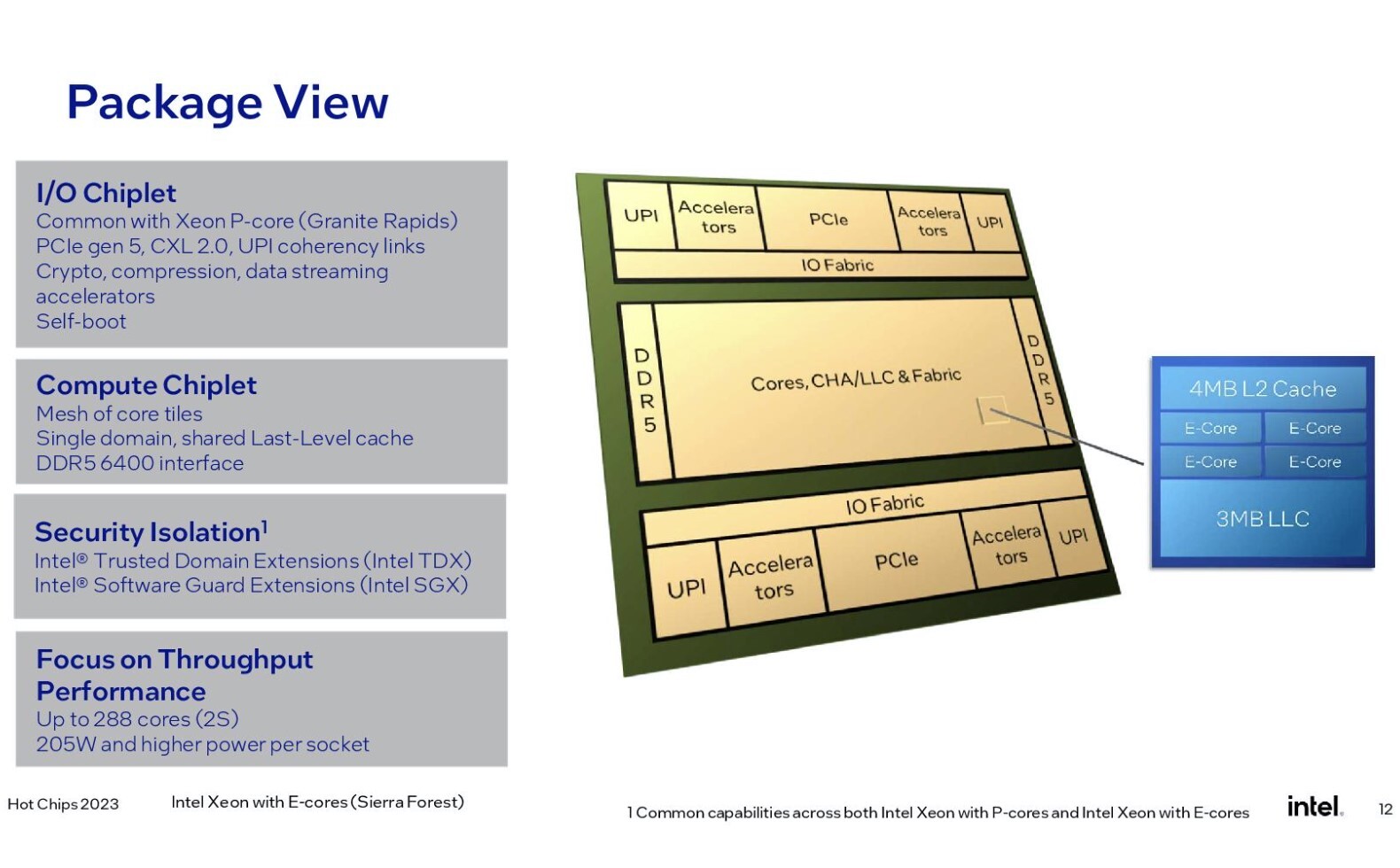
Intel Reports First-Quarter 2024 Financial Results

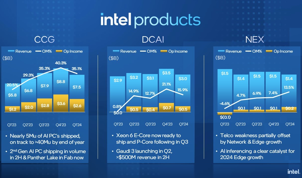
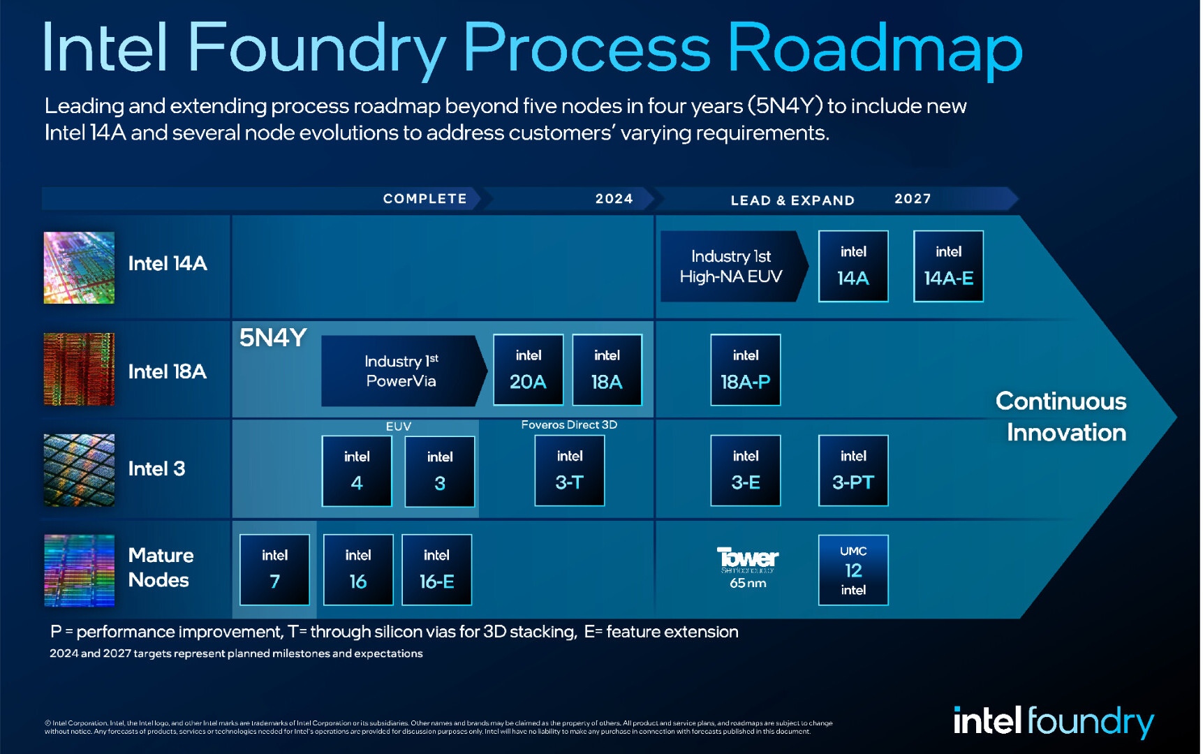
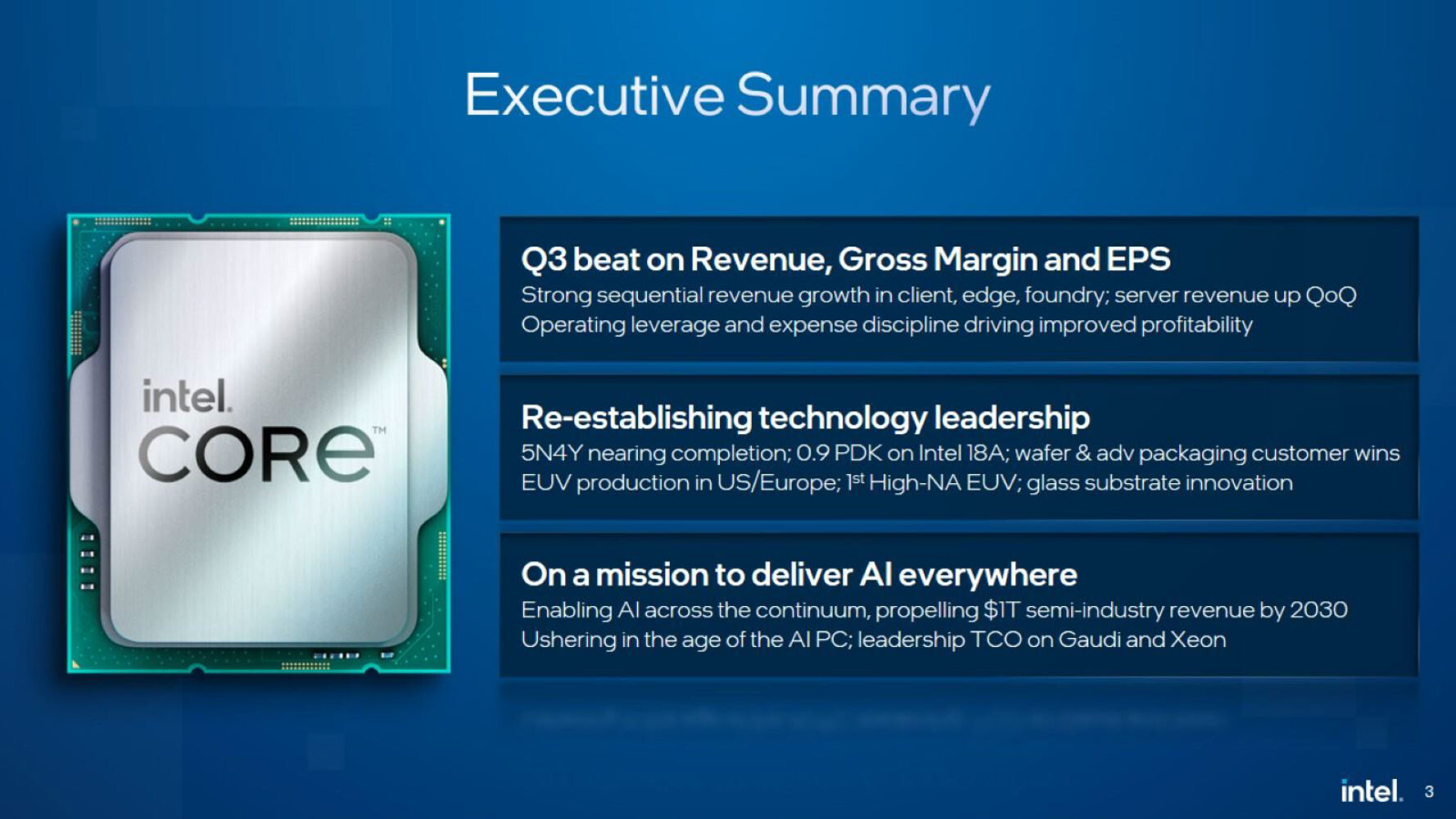
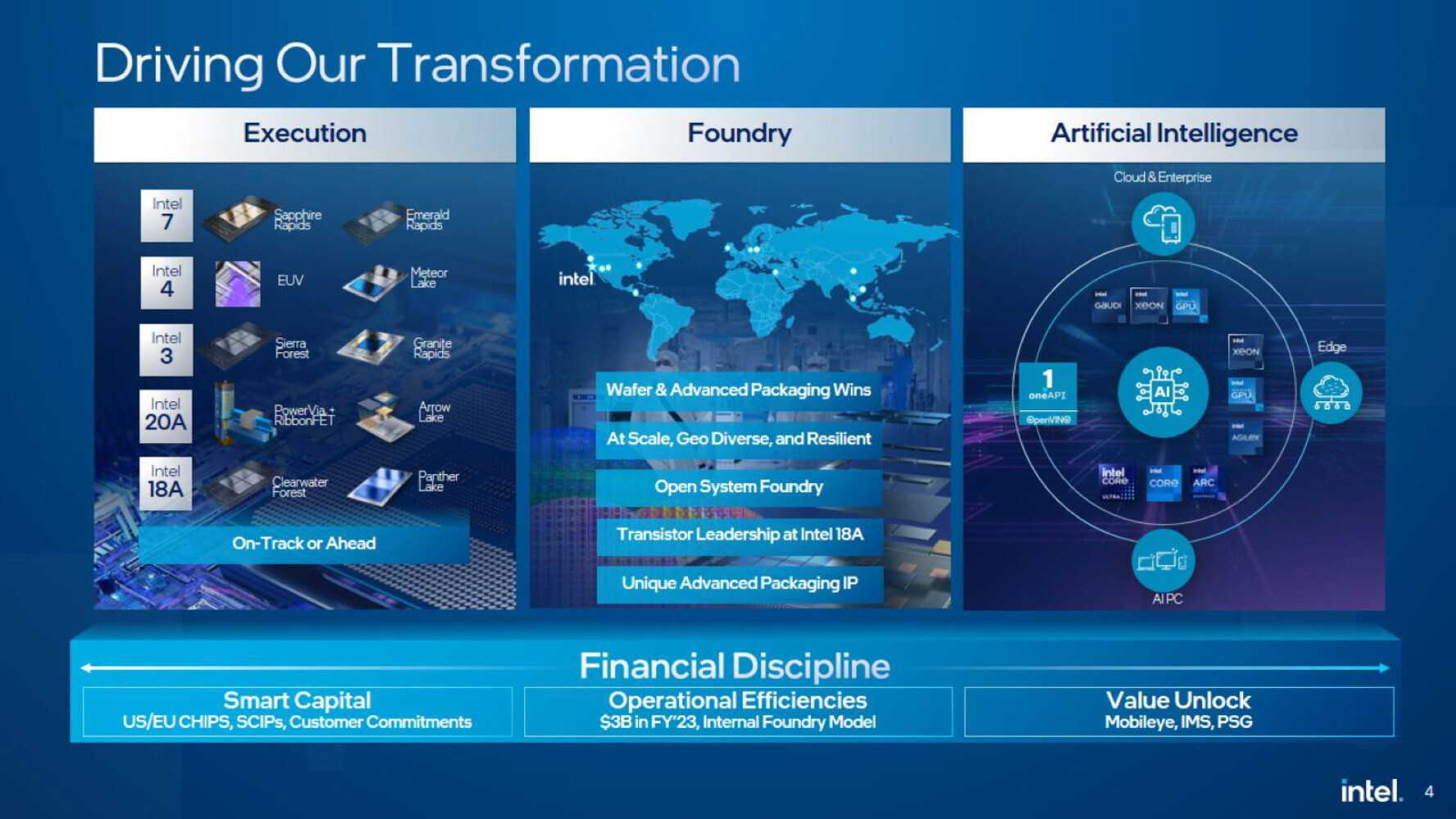
Intel Corporation today reported first-quarter 2024 financial results. "We are making steady progress against our priorities and delivered a solid quarter," said Pat Gelsinger, Intel CEO. "Strong innovation across our client, edge and data center portfolios drove double-digit revenue growth in Intel Products. With Intel 3 in high-volume production, leading-edge semiconductors are being manufactured in the U.S. for the first time in almost a decade and we are on track to regain process leadership next year as we grow Intel Foundry. We are confident in our plans to drive sequential growth throughout the year as we accelerate our AI solutions and maintain our relentless focus on execution, operational discipline and shareholder value creation in a dynamic market."

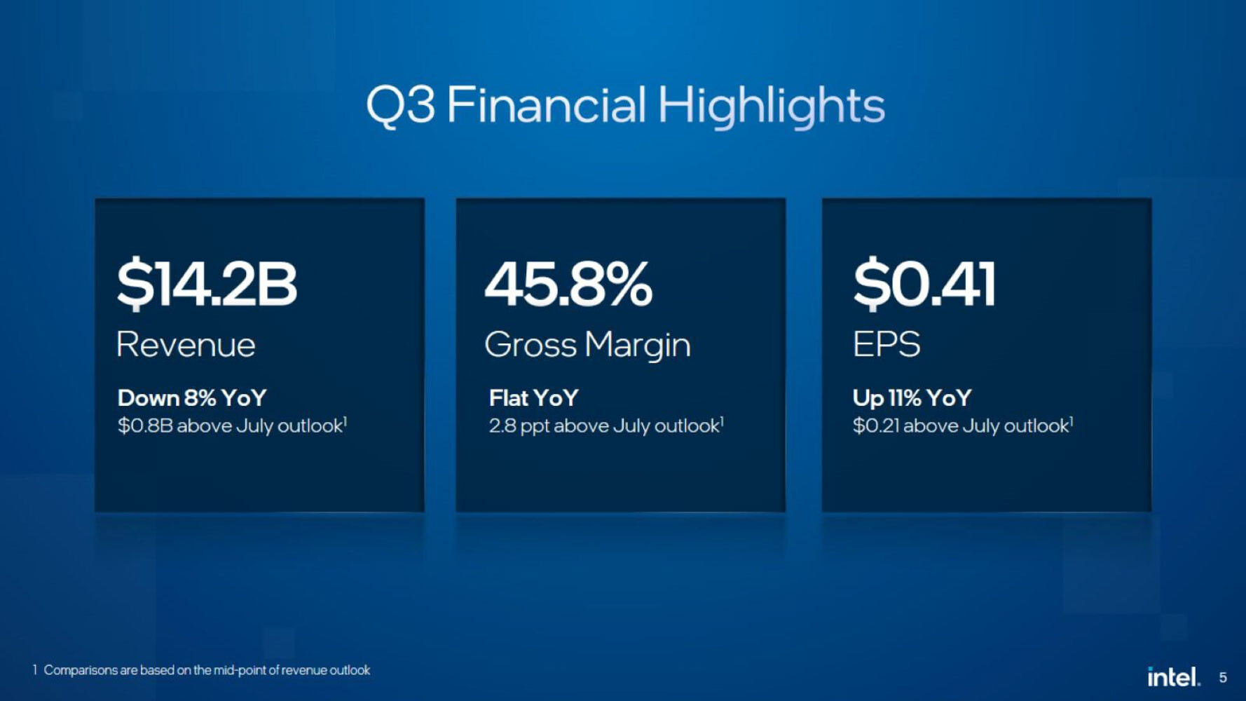
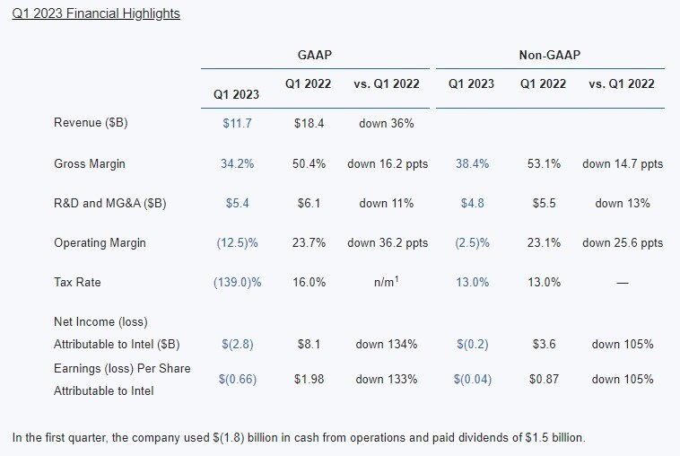
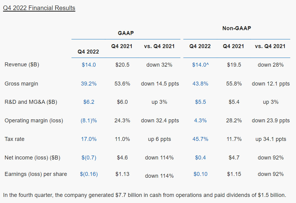
"Q1 revenue was in line with our expectations, and we delivered non-GAAP EPS above our guidance, driven by better-than-expected gross margins and strong expense discipline," said David Zinsner, Intel CFO. "Our new foundry operating model, which provides greater transparency and accountability, is already driving better decision-making across the business. Looking ahead, we expect to deliver year-over-year revenue and non-GAAP EPS growth in fiscal year 2024, including roughly 200 basis points of full-year gross margin improvement." In the first quarter, the company used $1.2 billion in cash from operations and paid dividends of $0.5 billion.

Intel Xeon "Granite Rapids-SP" 80-core Engineering Sample Leaked

A CPU-Z screenshot has been shared by YuuKi_AnS—the image contains details about an alleged next-gen Intel Xeon Scalable processor engineering sample (ES). The hardware tipster noted in (yesterday's post) that an error had occurred in the application's identification of this chunk of prototype silicon. CPU-Z v2.09 has recognized the basics—an Intel Granite Rapids-SP processor that is specced with 80 cores, 2.5 GHz max frequency, a whopping 672 MB of L3 cache, and a max. TDP rating of 350 W. The counting of 320 threads seems to be CPU-Z's big mistake here—previous Granite Rapids-related leaks have not revealed Team Blue's Hyper-Threading technology producing such impressive numbers.

The alleged prototype status of this Xeon chip is very apparent in CPU-Z's tracking of single and multi-core performance—the benchmark results are really off the mark, when compared to finalized current-gen scores (produced by rival silicon). Team Blue's next-gen Xeon series is likely positioned to catch up with AMD EPYC's deployment of large core counts—"Granite Rapids" has been linked to the Intel 3 foundry node, reports from last month suggest that XCC-type processors could be configured with "counts going up to 56-core/112-threads." Micron is prepping next-gen "Tall Form Factor" memory modules, designed with future enterprise processor platforms in mind—including Intel's Xeon Scalable "Granite Rapids" family. Industry watchdogs posit that Team Blue will be launching this series in the coming months.

Intel Announces Intel 14A (1.4 nm) and Intel 3T Foundry Nodes, Launches World's First Systems Foundry Designed for the AI Era

Intel Corp. today launched Intel Foundry as a more sustainable systems foundry business designed for the AI era and announced an expanded process roadmap designed to establish leadership into the latter part of this decade. The company also highlighted customer momentum and support from ecosystem partners - including Synopsys, Cadence, Siemens and Ansys - who outlined their readiness to accelerate Intel Foundry customers' chip designs with tools, design flows and IP portfolios validated for Intel's advanced packaging and Intel 18A process technologies.

The announcements were made at Intel's first foundry event, Intel Foundry Direct Connect, where the company gathered customers, ecosystem companies and leaders from across the industry. Among the participants and speakers were U.S. Secretary of Commerce Gina Raimondo, Arm CEO Rene Haas, Microsoft CEO Satya Nadella, OpenAI CEO Sam Altman and others.

Intel Xeon "Granite Rapids" Wafer Pictured—First Silicon Built on Intel 3

Feast your eyes on the first pictures of an Intel "Granite Rapids" Xeon processor wafer, courtesy of Andreas Schilling with HardwareLuxx.de. This is Intel's first commercial silicon built on the new Intel 3 foundry node, which is expected to be the company's final silicon fabrication node to implement FinFET technology; before the company switches to Nanosheets with the next-generation Intel 20A. Intel 3 offers transistor densities and performance competitive to TSMC N3 series, and Samsung 3GA series nodes.

The wafer contains square 30-core tiles, two of which make up a "Granite Rapids-XCC" processor, with CPU core counts going up to 56-core/112-threads (two cores left unused per tile for harvesting). Each of the 30 cores on the tile is a "Redwood Cove" P-core. In comparison, the current "Emerald Rapids" Xeon processor uses "Raptor Cove" cores, and is built on the Intel 7 foundry node. Intel is planning to overcome the CPU core-count deficit to AMD EPYC, including the upcoming EPYC "Turin" Zen 5 processors with their rumored 128-core/256-thread counts, by implementing several on-silicon fixed-function accelerators that speed up popular kinds of server workloads. The "Redwood Cove" core is expected to be Intel's first IA core to implement AVX10 and APX.

Report: Intel Seeks $2 Billion in Funding for Ireland Fab 34 Expansion

According to a Bloomberg report, Intel is seeking to raise at least $2 billion in equity funding from investors for expanding its fabrication facility in Leixlip, Ireland, known as Fab 34. The chipmaker has hired an advisor to find potential investors interested in providing capital for the project. Fab 34 is currently Intel's only chip plant in Europe that uses cutting-edge extreme ultraviolet (EUV) lithography. It produces processors on the Intel 4 process node, including compute tiles for Meteor Lake client CPUs and expected future Xeon data center chips. While $2 billion alone cannot finance the construction of an entirely new fab today, it can support meaningful expansion or upgrades of existing capacity. Intel likely aims to grow Fab 34's output and/or transition it to more advanced 3 nm-class technologies like Intel 3, Intel 20A, or Intel 18A.

Expanding production aligns with Intel's needs for its own products and its Intel Foundry Services business, providing contract manufacturing. Intel previously secured a $15 billion investment from Brookfield Infrastructure for its Arizona fabs in exchange for a 49% stake, demonstrating the company's willingness to partner to raise capital for manufacturing projects. The Brookfield deal also set a precedent of using outside financing to supplement Intel's own spending budget. It provided $15 billion in effectively free cash flow Intel can redirect to other priorities like new fabs without increasing debt. Intel's latest fundraising efforts for the Ireland site follow a similar equity investment model that leverages outside capital to support its manufacturing expansion plans. Acquiring High-NA EUV machinery for manufacturing is costly, as these machines can reach up to $380 million alone.

Intel, Marvell, and Synopsys to Showcase Next-Gen Memory PHY IP Capable of 224 Gbps on 3nm-class FinFET Nodes

The sneak peeks from the upcoming IEEE Solid State Circuit Conference continues, as the agenda items unveil interesting tech that will be either unveiled or demonstrated there. Intel, Synopsys, and Marvell, are leading providers of DRAM physical layer interface (PHY) IP. Various processor, GPU, and SoC manufacturers license PHY and memory controller IP from these companies, to integrate with their designs. All three companies are ready with over 200 Gbps around the 2.69 to 3 petajoule per bit range. This energy cost is as important as the data-rate on offer; as it showcases the viability of the PHY for a specific application (for example, a smartphone SoC has to conduct its memory sub-system at a vastly more constrained energy budget compared to an HPC processor).

Intel is the first in the pack to showcase a 224 Gbps sub-picojoule/bit PHY transmitter that supports PAM4 and PAM6 signaling, and is designed for 3 nm-class FinFET foundry nodes. If you recall, Intel 3 will be the company's final FinFET node before it transitions to nanosheets with the Intel 20A node. At the physical layer, all digital memory signal is analogue, and Intel's IP focuses on the DAC aspect of the PHY. Next up, is a somewhat similar transceiver IP by Synopsys. This too claims 224 Gbps speeds at 3 pJ/b, but at a 40 dB insertion loss; and is designed for 3 nm class FinFET nodes such as the TSMC N3 family and Intel 3. Samsung's 3 nm node uses the incompatible GAAFET technology for its 3 nm EUV node. Lastly, there's Marvell, with a 212 Gb/s DSP-based transceiver for optical direct-detect applications on the 5 nm FinFET nodes, which is relevant for high speed network switching fabrics.

Intel Reports Third-Quarter 2023 Financial Results

Intel Corporation today reported third-quarter 2023 financial results. "We delivered a standout third quarter, underscored by across-the-board progress on our process and product roadmaps, agreements with new foundry customers, and momentum as we bring AI everywhere," said Pat Gelsinger, Intel CEO. "We continue to make meaningful progress on our IDM 2.0 transformation by relentlessly advancing our strategy, rebuilding our execution engine and delivering on our commitments to our customers."

David Zinsner, Intel CFO, said, "Our results exceeded expectations for the third consecutive quarter, with revenue above the high end of our guidance and EPS benefiting from strong operating leverage and expense discipline. As demonstrated by our recent portfolio actions, we are highly focused on being great allocators of our owners' capital and unlocking value for shareholders."

Intel Demoes Core "Lunar Lake" Processor from Two Generations Ahead

Intel at the 2023 InnovatiON event surprised audiences with a live demo of a reference notebook powered by a Core "Lunar Lake" processor. What's surprising about this is that "Lunar Lake" won't come out until 2025 (at least), and succeeds not just the upcoming "Meteor Lake" architecture, but also its succeeding "Arrow Lake," which debuts in 2024. Intel is expected to debut "Meteor Lake" some time later this year. What's also surprising is that Intel has proven that the Intel 18A foundry node works. The Compute tile of "Lunar Lake" is expected to be based on Intel 18A, which is four generations ahead of the current Intel 7, which will be succeeded by Intel 4, Intel 3, and Intel 20A along the way.

The demo focused on the generative AI capabilities of Intel's third generation NPU, the hardware backend of AI Boost. Using a local session of a tool similar to Stable Diffusion, the processor was made to generate the image of a giraffe wearing a hat; and a GPT program was made to pen the lyrics of a song in the genre of Taylor Swift from scratch. Both tasks were completed on stage using the chip's NPU, and in timeframes you'd normally expect from discrete AI accelerators or cloud-based services.

Intel 288 E-core Xeon "Sierra Forest" Out to Eat AMD EPYC Bergamo's Lunch

Intel at the 2023 InnovatiON event unveiled a 288-core extreme core-count variant of the Xeon "Sierra Forest" processor for high-density servers for scale-out, cloud-native environments. It succeeds the current 144-core model. "Sierra Forest" is a server processor based entirely on efficiency cores, or E-cores, based on the "Sierra Glen" core microarchitecture, a server-grade derivative of "Crestmont," Intel's second-generation E-core that's making a client debut with "Meteor Lake."

Xeon "Sierra Forest" is a chiplet-based processor, much like "Meteor Lake" and the upcoming "Emerald Rapids" server processor. It features a total of five tiles—two Compute tiles, two I/O tiles, and a base tile (interposer). Each of the two Compute tiles is built on the Intel 3 foundry node, a more advanced node than Intel 4, featuring higher-density libraries, and an undisclosed performance/Watt increase. Each tile has 36 "Sierra Glen" E-core clusters, 108 MB of shared L3 cache, 6-channel (12 sub-channel) DDR5 memory controllers, and Foveros tile-to-tile interfaces.

Intel Foundry Services and Tower Semiconductor Announce New US Foundry Agreement

Intel Foundry Services (IFS) and Tower Semiconductor, a leading foundry for analog semiconductor solutions, today announced an agreement where Intel will provide foundry services and 300 mm manufacturing capacity to help Tower serve its customers globally. Under the agreement, Tower will utilize Intel's advanced manufacturing facility in New Mexico. Tower will invest up to $300 million to acquire and own equipment and other fixed assets to be installed in the New Mexico facility, providing a new capacity corridor of over 600,000 photo layers per month for Tower's future growth, enabling capacity to support forecasted customer demand for 300 mm advanced analog processing.

This agreement demonstrates the commitment from both Intel and Tower to expand their respective foundry footprints with unparalleled solutions and scaled capabilities. Intel will manufacture Tower's highly differentiated 65-nanometer power management BCD (bipolar-CMOS-DMOS) flows, among other flows at Intel's Fab 11X in Rio Rancho, New Mexico.

Samsung Claims Higher 3 nm Yields than TSMC

Competition between Samsung and TSMC in the 4 nm and 3 nm foundry process markets is about to heat up, with the Korean foundry claiming yields competitive to those of TSMC, according to a report in the Kukmin Ilbo, a Korean daily newspaper. 4 nm is the final silicon fabrication process to use the FinFET technology that powered nodes ranging between 16 nm to 4 nm. Samsung Foundry is claiming 4 nm wafer yields of 75%, against the 80% yields figure put out by TSMC. 4 nm powers several current-generation mobile SoCs, PC processors, and more importantly, the GPUs driving the AI gold-rush.

Things get very interesting with 3 nm, the node that debuts GAA-FET (gates all around FET) technology. Here, Samsung claims to offer higher yields than TSMC, with its 3 nm GAA node clocking 60% yields, against 55% put out by TSMC. Samsung was recently bitten by a scandal where its engineers allegedly falsified yields figures to customers to score orders, which had a cascading effect on the volumes and competitiveness of their customers. We're inclined to think that Samsung has taken lessons and is more careful with the yields figures being reported in the press. Meanwhile, Intel Foundry Services competes with the Intel 3 node, which is physically 7 nm FinFET, but with electrical characteristics comparable to those of 3 nm.

Intel Reports First-Quarter 2023 Financial Results: Client and Server Businesses Down 38-39% Each

Intel Corporation today reported first-quarter 2023 financial results. "We delivered solid first-quarter results, representing steady progress with our transformation," said Pat Gelsinger, Intel CEO. "We hit key execution milestones in our data center roadmap and demonstrated the health of the process technology underpinning it. While we remain cautious on the macroeconomic outlook, we are focused on what we can control as we deliver on IDM 2.0: driving consistent execution across process and product roadmaps and advancing our foundry business to best position us to capitalize on the $1 trillion market opportunity ahead."

David Zinsner, Intel CFO, said, "We exceeded our first-quarter expectations on the top and bottom line, and continued to be disciplined on expense management as part of our commitment to drive efficiencies and cost savings. At the same time, we are prioritizing the investments needed to advance our strategy and establish an internal foundry model, one of the most consequential steps we are taking to deliver on IDM 2.0."

Intel Foundry Services Allegedly Working on Test Chips for 43 Potential Customers

A new story is making the rounds, citing Wang Rui, chair Intel China, in the media in both China and Taiwan, claiming that Intel is working on test chips for as many as 43 potential customers for Intel Foundry Services (IFS). At least seven of those potential customers are said to be from the top 10 foundry clients globally. This sounds a bit too good to be true, considering that IFS has as yet to prove that they can deliver on their promises.

Furthermore, Wang Rui is meant to have gone on record, saying that IFS has taped out products on both its 20A and 18A nodes. Exactly what these products are, wasn't divulged, but as the 18A node isn't expected to go into mass production until the second half of 2024, this sounds a little bit too good to be true. What makes this even less believable is that the Intel 4 node is only set to go into mass production in the second half this year and before Intel moves to its Ångström nodes, the company still has to deliver on its Intel 3 node. The Intel China chair is also reportedly confident that Intel will be returning to a leading foundry position by 2025.

Intel LGA-7529 Socket for "Sierra Forest" Xeon Processors Pictured

Intel's upcoming LGA-7529 socket designed for next-generation Xeon processors has been pictured, thanks to Yuuki_Ans and Hassan Mujtaba. According to the latest photos, we see the massive LGA-7529 socket with an astonishing 7,529 pins placed inside of a single socket. Made for Intel's upcoming "Birch Stream" platform, this socket is going to power Intel's next-generation "Sierra Forest" Xeon processors. With Sierra Forest representing a new way of thinking about Xeon processors, it also requires a special socket. Built on Intel 3 manufacturing process, these Xeon processors use only E-cores in their design to respond to AMD EPYC Bergamo with Zen4c.

The Intel Xeon roadmap will split in 2024, where Sierra Forest will populate dense and efficient cloud computing with E-cores, while its Granite Rapids sibling will power high-performance computing using P-cores. This interesting split will be followed by the new LGA-7529 socket pictured below, which is a step up from Intel's current LGA-4677 socket with 4677 pins used for Sapphire Rapids. With higher core densities and performance targets, the additional pins are likely to be mostly power/ground pins, while the smaller portion is picking up the additional I/O of the processor.

20:20 UTC: Updated with motherboard picture of dual-socket LGA-7529 system, thanks to findings of @9550pro lurking in the Chinese forums.

Intel Foundry Services Onboards a Fabless Customer, Deal Expected to Fetch over $4 Billion

Intel Foundry Services, the semiconductor foundry business of Intel, has onboarded an undisclosed fabless customer, the company disclosed in its Q4-2022 Financial Results presentation. This signals that the company wants to serve the semiconductor manufacturing industry beyond its own products, and scale up to demands, just like TSMC, UMC, Samsung Foundry, or other such semiconductor foundries do. The customer is looking to build chips on the Intel 3 foundry-node, which is rumored to offer performance/Watt and transistor-density figures comparable to TSMC 4N (4 nm EUV). Intel will extensively use Tower Semiconductor's silicon fabrication IP in the deal. Throughout its manufacturing lifecycle (from risk production to mass-production and completion), the deal is expected by Intel to generate over $4 billion in revenue for the company.
Image Courtesy: VideoCardz

Intel Xeon "Sapphire Rapids" to be Quickly Joined by "Emerald Rapids," "Granite Rapids," and "Sierra Forest" in the Next Two Years

Intel's server processor lineup led by the 4th Gen Xeon Scalable "Sapphire Rapids" processors face stiff competition from AMD 4th Gen EPYC "Genoa" processors that offer significantly higher multi-threaded performance per Watt on account of a higher CPU core-count. The gap is only set to widen, as AMD prepares to launch the "Bergamo" processor for cloud data-centers, with core-counts of up to 128-core/256-thread per socket. A technologically-embattled Intel is preparing quick counters as many as three new server microarchitecture launches over the next 23 months, according to Intel, in its Q4-2022 Financial Results presentation.

The 4th Gen Xeon Scalable "Sapphire Rapids," with a core-count of up to 60-core/120-thread, and various application-specific accelerators, witnessed a quiet launch earlier this month, and is shipping to Intel customers. The company says that it will be joined by the Xeon Scalable "Emerald Rapids" architecture in the second half of 2023; followed by "Granite Rapids" and "Sierra Forest" in 2024. Built on the same LGA4677 package as "Sapphire Rapids," the new "Emerald Rapids" MCM packs up to 64 "Raptor Cove" CPU cores, which support higher clock-speeds, higher memory speeds, and introduce the new Intel Trust Domain Extensions (TDX) instruction-set. The processor retains the 8-channel DDR5 memory interface, but with higher native memory speeds. The chip's main serial interface is a PCI-Express Gen 5 root-complex with 80 lanes. The processor will be built on the last foundry-level refinement of the Intel 7 node (10 nm Enhanced SuperFin); many of these refinements were introduced with the company's 13th Gen Core "Raptor Lake" client processors.

Intel Reports Fourth-Quarter and Full-Year 2022 Financial Results, Largest Loss in Years

Intel Corporation today reported fourth-quarter and full-year 2022 financial results. The company also announced that its board of directors has declared a quarterly dividend of $0.365 per share on the company's common stock, which will be payable on March 1, 2023, to shareholders of record as of February 7, 2023.

"Despite the economic and market headwinds, we continued to make good progress on our strategic transformation in Q4, including advancing our product roadmap and improving our operational structure and processes to drive efficiencies while delivering at the low-end of our guided range," said Pat Gelsinger, Intel CEO. "In 2023, we will continue to navigate the short-term challenges while striving to meet our long-term commitments, including delivering leadership products anchored on open and secure platforms, powered by at-scale manufacturing and supercharged by our incredible team."

Intel Reports Third-Quarter 2022 Financial Results

Intel Corporation today reported third-quarter 2022 financial results. "Despite the worsening economic conditions, we delivered solid results and made significant progress with our product and process execution during the quarter," said Pat Gelsinger, Intel CEO. "To position ourselves for this business cycle, we are aggressively addressing costs and driving efficiencies across the business to accelerate our IDM 2.0 flywheel for the digital future."

"As we usher in the next phase of IDM 2.0, we are focused on embracing an internal foundry model to allow our manufacturing group and business units to be more agile, make better decisions and establish a leadership cost structure," said David Zinsner, Intel CFO. "We remain committed to the strategy and long-term financial model communicated at our Investor Meeting."

Intel Joins DARPA's Space-BACN to Accelerate Inter-Satellite Communications

he U.S. Defense Advanced Research Projects Agency (DARPA) has selected Intel for Phase 1 of the Space-Based Adaptive Communications Node (Space-BACN) program, which aims to create a low-cost, reconfigurable optical communications terminal that will translate information between diverse satellite constellations. A Space-BACN satellite terminal will enable communications between satellite constellations, enabling data to be sent anywhere around the planet at the speed of light.

DARPA is planning for a future where tens of thousands of satellites from multiple private sector organizations deliver broadband services from low earth orbit (LEO). The goal of Space-BACN is to create an "internet" of satellites, enabling seamless communication between military/government and commercial/civil satellite constellations. The program will facilitate collaboration among partners to ensure that the terminal being designed is reconfigurable to provide interoperability among the participating constellation providers.

Intel Updates Technology Roadmap with Data Center Processors and Game Streaming Service

At Intel's 2022 Investor Meeting, Chief Executive Officer Pat Gelsinger and Intel's business leaders outlined key elements of the company's strategy and path for long-term growth. Intel's long-term plans will capitalize on transformative growth during an era of unprecedented demand for semiconductors. Among the presentations, Intel announced product roadmaps across its major business units and key execution milestones, including: Accelerated Computing Systems and Graphics, Intel Foundry Services, Software and Advanced Technology, Network and Edge, Technology Development, More: For more from Intel's Investor Meeting 2022, including the presentations and news, please visit the Intel Newsroom and Intel.com's Investor Meeting site.

Intel Expects New US Fab Investment to Cost $60 to $120 billion

In an interview with the Washington Post, Intel CEO Pat Gelsinger shared some details on the company's plans to expand its foundry operations in the US. As part of the company's IDM 2.0 plan, the company aims to construct a new cutting edge fabrication complex that will cover both wafer manufacturing and advanced packaging technologies. While the final factory location still hasn't been disclosed, the company said it plans to build the complex in close proximity to universities - a way to facilitate the hiring process of qualified personnel and, perhaps, of establishing joint research and development. Intel expects this foundry complex to cost between $60 and $120 billion.
Intel CEO Pat GelsingerWe are looking broadly across the U.S.. This would be a very large site, so six to eight fab modules, and at each of those fab modules, between 10- and $15 billion. It's a project over the next decade on the order of $100 billion of capital, 10,000 direct jobs. 100,000 jobs are created as a result of those 10,000, by our experience. So, essentially, we want to build a little city."

Intel Rebadges 10nm Enhanced SuperFin Node as "Intel 7," Invents Other Creative Node Names

Intel, in a move comparable to its competitors' Performance Rating system from the 1990s, has invented a new naming scheme for its in-house foundry nodes to claim technological parity with contemporaries such as TSMC and Samsung, that are well into the sub-10 nm class. Back in the i586 era, when Intel's competitors such as AMD and Cyrix, couldn't keep up with its clock-speeds yet found their chips to be somewhat competitive, they invented the PR (processor rating) system, with a logical number attempting to denote parity with an Intel processor's clock-speed. For example, a PR400 processor rating meant that the chip rivaled a Pentium II 400 MHz (which it mostly didn't). The last that the PR system made sense was with the final generation of single-core performance chips, Pentium 4 and Athlon XP, beyond which, the introduction of multi-core obfuscated the PR system. A Phenom X4 9600 processor didn't mean performance on par with a rival Intel chip running at an impossible 9.60 GHz.

Intel's new foundry naming system sees its 10 nm Enhanced SuperFin node re-badge as "Intel 7." The company currently builds 11th Gen Core "Tiger Lake" processors on the 10 nm SuperFin node, and is expected to build its upcoming 12th Gen Core "Alder Lake" chips on its refinement, the 10 nm Enhanced SuperFin, which will now be referred to as "Intel 7." The company is careful to avoid using the nanometer unit next to the number, instead signaling the consumer that the node somehow offers transistor density and power characteristics comparable to a 7 nm node. Intel 7 offers a 10-15 percent performance/Watt gain over 10 nm SuperFin, and is already in volume production, with a debut within 2021 with "Alder Lake."

Intel Accelerates Packaging and Process Innovations

Intel Corporation today revealed one of the most detailed process and packaging technology roadmaps the company has ever provided, showcasing a series of foundational innovations that will power products through 2025 and beyond. In addition to announcing RibbonFET, its first new transistor architecture in more than a decade, and PowerVia, an industry-first new backside power delivery method, the company highlighted its planned swift adoption of next-generation extreme ultraviolet lithography (EUV), referred to as High Numerical Aperture (High NA) EUV. Intel is positioned to receive the first High NA EUV production tool in the industry.

"Building on Intel's unquestioned leadership in advanced packaging, we are accelerating our innovation roadmap to ensure we are on a clear path to process performance leadership by 2025," Intel CEO Pat Gelsinger said during the global "Intel Accelerated" webcast. "We are leveraging our unparalleled pipeline of innovation to deliver technology advances from the transistor up to the system level. Until the periodic table is exhausted, we will be relentless in our pursuit of Moore's Law and our path to innovate with the magic of silicon."
Return to Keyword Browsing
Apr 29th, 2024 16:56 EDT change timezone

New Forum Posts

Popular Reviews

Controversial News Posts