Thursday, August 19th 2021

Intel Xe HPG Graphics Architecture and Arc "Alchemist" GPU Detailed
It's happening, Intel is taking a very pointy stab at the AAA gaming graphics market, taking the fight to NVIDIA GeForce and AMD Radeon. The Arc "Alchemist" discrete GPU implements the Xe HPG (high performance gaming) graphics architecture, and offers full DirectX 12 Ultimate compatibility. It also offers contemporary features gamers want, such as XeSS, an AI-supersampling feature rivaling DLSS and FSR. There's a lot more to the Xe HPG architecture than being a simple a scale-up from the Xe LP-based iGPUs found in today's "Tiger Lake" processors.
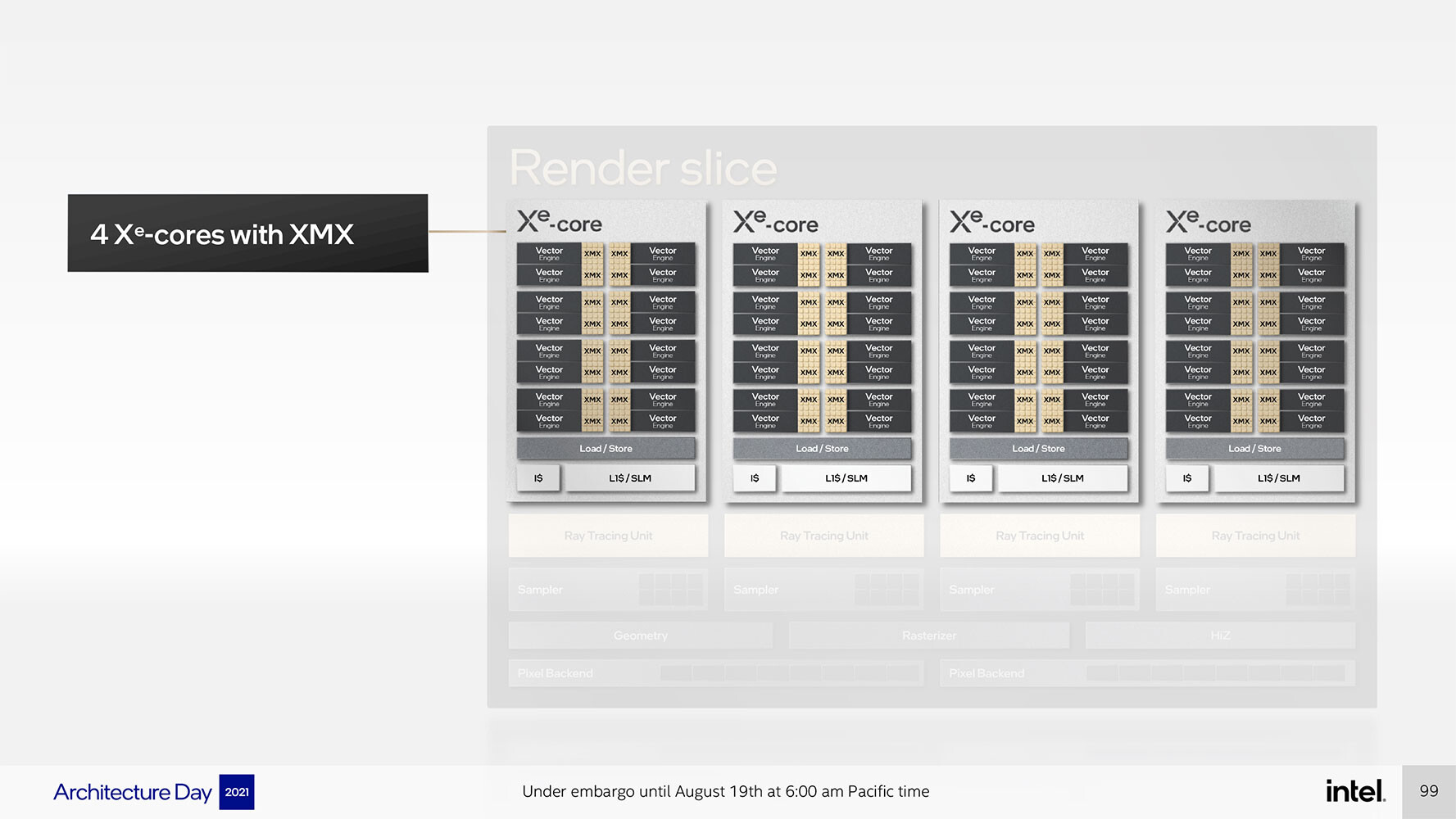
Just like Compute Units on AMD GPUs, and Streaming Multiprocessors on NVIDIA, Intel designed a scalable hierarchical compute hardware structure for Xe HPG. It begins with the Xe-core, an indivisible compute building block that contains 16 each of 256-bit vector engines and 1024-bit matrix engines. combined with basic load/store hardware and an L1 cache. The vector unit here is interchangeable with the execution unit, and the Xe-core contains 16 of these. The Render Slice is a collective of four Xe-cores, four Raytracing Units; and other common fixed-function hardware that include the geometry pipeline, rasterization pipeline, samplers, and pixel-backends. The Raytracing Units contain fixed-function hardware for bounding-box intersection, ray traversal, and triangle intersection.


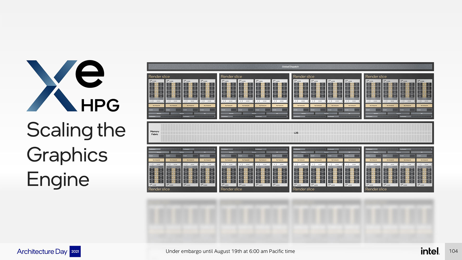
 Moving a level up from the Render Slice, we see a Global Dispatch processor, and the GPU's memory fabric, which begins with an L2 cache. This is where Intel can scale up its GPUs. The 6 nm "Alchemist" silicon features eight Render Slices sharing the memory subsystem and Global Dispatch. Intel can carve out variants by toggling entire Render Slices, or perhaps even individual Xe-cores. With 16 EUs per Xe-core, 4 Xe-cores per Render Slice, and 8 Render Slices, we arrive at 512 execution units, or 4,096 programmable shaders.


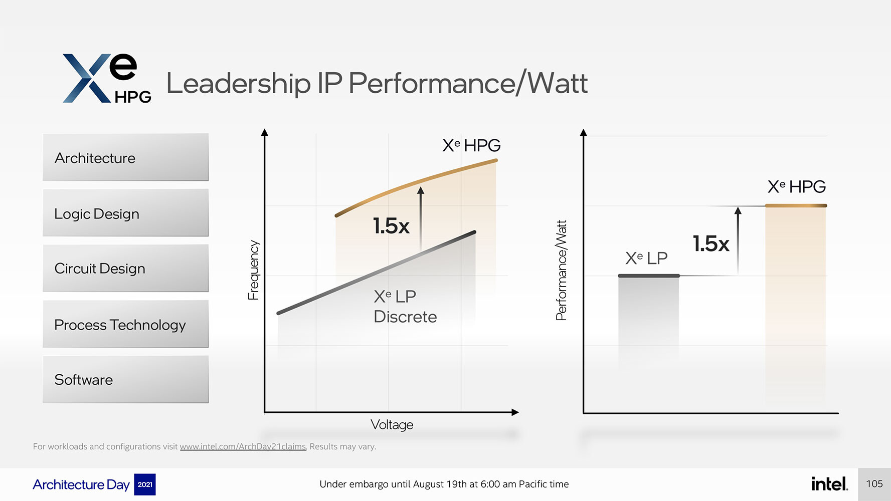
 Given that Xe HPG is being designed for the TSMC N6 (6 nm) silicon fabrication node, Intel claims a 50% performance/Watt gain over Xe LP solutions built on Intel's own 10 nm SuperFin nodes, such as the DG1 Iris Xe MAX. As a performance discrete GPU, "Alchemist" enjoys a much larger power budget, and hence operates at much higher frequencies for the available hardware.
 Although not mentioned in the Intel presentation, it's been extensively reported that "Alchemist" (or DG2) features a 256-bit wide GDDR6 memory interface. The company is yet to determine memory size, but given the memory speeds available in the market (14 Gbps, 16 Gbps, and 18 Gbps), the memory bandwidth can end up anywhere between 448 GB/s to 576 GB/s.
Armed with as many as 512x 1024-bit Matrix cores backed by Xe Matrix extensions "Alchemist" is expected to be an AI processing powerhouse, with Intel leveraging them both for the XeSS performance enhancement feature, as well as other real-time rendering applications, such as de-noising for the raytracing pipeline. Intel Arc "Alchemist" is expected to see a market release in Q1 2022. The company is ready with a roadmap with at least three of its successors, the Xe2 "Battlemage," Xe3 "Celestial," and XeNext "Druid." With no time-scale mentioned in the slide, we don't know if Intel is executing one architecture every year.
Just like Compute Units on AMD GPUs, and Streaming Multiprocessors on NVIDIA, Intel designed a scalable hierarchical compute hardware structure for Xe HPG. It begins with the Xe-core, an indivisible compute building block that contains 16 each of 256-bit vector engines and 1024-bit matrix engines. combined with basic load/store hardware and an L1 cache. The vector unit here is interchangeable with the execution unit, and the Xe-core contains 16 of these. The Render Slice is a collective of four Xe-cores, four Raytracing Units; and other common fixed-function hardware that include the geometry pipeline, rasterization pipeline, samplers, and pixel-backends. The Raytracing Units contain fixed-function hardware for bounding-box intersection, ray traversal, and triangle intersection.


Armed with as many as 512x 1024-bit Matrix cores backed by Xe Matrix extensions "Alchemist" is expected to be an AI processing powerhouse, with Intel leveraging them both for the XeSS performance enhancement feature, as well as other real-time rendering applications, such as de-noising for the raytracing pipeline.

14 Comments on Intel Xe HPG Graphics Architecture and Arc "Alchemist" GPU Detailed
You are discovering, unsurprisingly, that node names are incredibly misleading.
It is universal, sadly.
TMUs: 256
ROPs: 128
Compute units/SM Count/ Xe Cores: 32
RT Cores: 32
L1 Cache: ? KB
L2 Cache: ? MB
Memory Size: ? GB
Memory Type: GDDR6/X ?
Memory Bus: 256 bit ?
Bandwidth: 448 ~ 576 GB/s
-Spec wise, it's slightly less than a rx 6800 xt at 4608 vs 4096 shader (or 288 vs 256 TMUs)
-It will all depend on the gpu clocks the TSMC N6 will achieve, Intel is claiming 1.5x more than the Xe LP discrete; but we don't know 1.5x 1.1Ghz or 1.5Ghz...
-As for raytracing, it only has 32 RT cores, significantly less compared to 82 on Ampere and 80 on RDNA 2.0 but we don't know the performance of its RT core yet.
But now its claimed to have a 50% uplift going for TSMC 6nm which....well TSMC never claimed would be the improvement from such a relatively minor shrink.
But the real questions are:
- price
- form factors
- noise/heat/TDP
- feature set