Tuesday, September 19th 2023

Pat Gelsinger Says 3D Stacked Cache Tech Coming to Intel
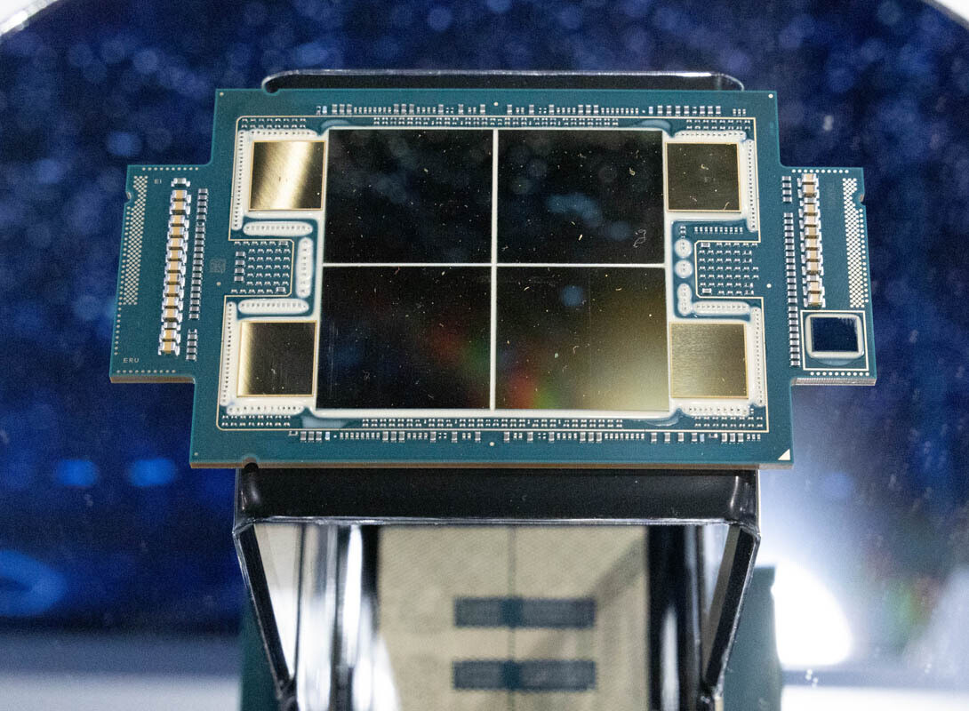
Intel CEO Pat Gelsinger, in the Q&A session of InnovatiON 2023 Day 1, confirmed that the company is developing 3D-stacked cache technology for its processors. The technology involves expanding the on-die last-level cache (L3 cache) of a processor with an additional SRAM die physically stacked on top, and bonded with the cache's high-bandwidth data fabric. The stacked cache operates at the same speed as the on-die cache, and so the combined cache size is visible to software as a single contiguous addressable block of cache memory.
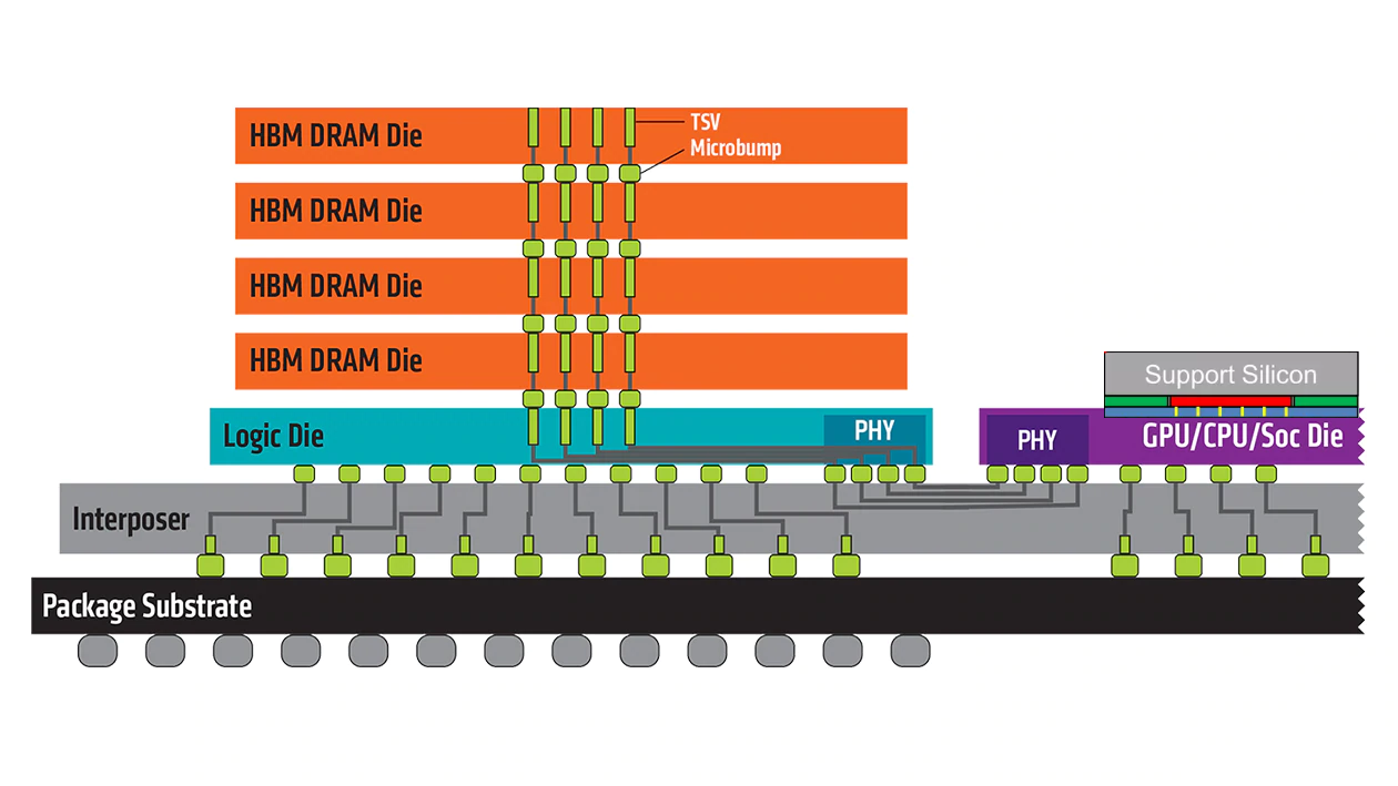
AMD has used 3D-stacked cache to good effect on its processors. On client processors such as the Ryzen X3D series, the cache provides significant gaming performance uplifts as the larger L3 cache makes more of the game's rendering data immediately accessible to the CPU cores; while on server processors such as EPYC "Milan-X" and "Genoa-X," the added cache provides significant uplifts to memory intensive compute workloads. Intel's approach to 3D-stacked cache will be different at the hardware level compared to AMD's, Gelsinger stated in his response. AMD's tech has been collaboratively developed with TSMC, and hinges on a TSMC-made SoIC packaging tech that facilitates high-density die-to-die wiring between the CCD and cache chiplet. Intel uses its own fabs for processor dies, and will have to use its own IP. "When you reference V-Cache, you're talking about a very specific technology that TSMC does with some of its customers as well. Obviously, we're doing that differently in our composition, right? And that particular type of technology isn't something that's part of Meteor Lake, but in our roadmap, you're seeing the idea of 3D silicon where we'll have cache on one die, and we'll have CPU compute on the stacked die on top of it, and obviously using EMIB that Foveros we'll be able to compose different capabilities," Gelsinger said.
"We feel very good that we have advanced capabilities for next-generation memory architectures, advantages for 3D stacking, for both little die, as well as for very big packages for AI and high-performance servers as well. So we have a full breadth of those technologies. We'll be using those for our products, as well as presenting it to the Foundry (IFS) customers as well," he added.
Intel recently provided an architecture deep-dive into its upcoming "Meteor Lake" client processor, in which its Foveros packaging tech and tile-to-tile interconnects allow the various tiles (chiplets) to work like a cohesive silicon. In particular, Intel appears to have solved the latency issues of having a the iGPU, CPU cores, and memory controllers on separate tiles.
Source:
Tom's Hardware
AMD has used 3D-stacked cache to good effect on its processors. On client processors such as the Ryzen X3D series, the cache provides significant gaming performance uplifts as the larger L3 cache makes more of the game's rendering data immediately accessible to the CPU cores; while on server processors such as EPYC "Milan-X" and "Genoa-X," the added cache provides significant uplifts to memory intensive compute workloads. Intel's approach to 3D-stacked cache will be different at the hardware level compared to AMD's, Gelsinger stated in his response. AMD's tech has been collaboratively developed with TSMC, and hinges on a TSMC-made SoIC packaging tech that facilitates high-density die-to-die wiring between the CCD and cache chiplet. Intel uses its own fabs for processor dies, and will have to use its own IP.
"We feel very good that we have advanced capabilities for next-generation memory architectures, advantages for 3D stacking, for both little die, as well as for very big packages for AI and high-performance servers as well. So we have a full breadth of those technologies. We'll be using those for our products, as well as presenting it to the Foundry (IFS) customers as well," he added.
Intel recently provided an architecture deep-dive into its upcoming "Meteor Lake" client processor, in which its Foveros packaging tech and tile-to-tile interconnects allow the various tiles (chiplets) to work like a cohesive silicon. In particular, Intel appears to have solved the latency issues of having a the iGPU, CPU cores, and memory controllers on separate tiles.
31 Comments on Pat Gelsinger Says 3D Stacked Cache Tech Coming to Intel
what is the point of innovation these days when people just copy you lol
Intel's approach is different BTW, and who cares, if it improves the product and improves efficiency like in AMD's case, bring it on.
TSMC is I hope making money off its 3dcache invention, if not, then they are a foolish company.
uspto.report/patent/app/20210374607
Also one of the person on that patent is my classmate and currently he seems to be employed by Intel.
There are older(now expired) patents from T.I. and Philips as well:
patents.google.com/patent/US6141235
patents.google.com/patent/US5953741A/en
EG1. Ok, someone beat me to it.No, just no.
TSMC even owns the name 3d.
3dfabric.tsmc.com/english/dedicatedFoundry/technology/3DFabric.htm
TSMC owns the packaging technology that enabled AMD to create 3D V-Cache, but AMD owns the actual 3D V-Cache design.
The two clearly collaborated to make it work, based on TSMC's packaging technology, as without it, AMD couldn't have made it.
The two are not the same though and TSMC doesn't actually make any "products" as such, so why would they be making cache wafers on their own and then sell it to someone who might want it? It makes zero sense, as that's not how TSMC operates. Then they would also be making Arm based chips or whatever and selling it to whoever wants them and they do not.
TSMC is a foundry, they design tech that their customers can leverage, they don't design chips or parts of chips.
Anandtech did a deep dive into this in 2021.
If it is so simple then Intel would have achieve this long ago, not wait for a couple gen and let AMD "steal" their thunder.
Intel is making a big deal out of this, I would assume there are some major engineering hurdle that they overcame.
Now, with All the Big Players getting in on 3D stacking Cache/Mem, I'm wondering if 'consumers' will see HBM on CPUs and GPUs(again)
My bet:
The Generation after the immediately-inbound generation, we'll see HBM products in the consumer marketspace.
Not just Intel/AMD/nVidia, either; I'm thinking HBM-equipped SoCs for mobile devices, and considerations for future handheld PCs and Consoles.
HBM demand is higher than ever right now in Accelerators cards espeically with the whole AI craze going on.
If yields are that high, and interposers are popping up across products we'd never thought of; meaning, better manufacturing/assembly yields...
At least historically, the consumer segment (eventually) gets the scraps from well-developed and high-yielding new technologies.
However, you do have a point.
If AI/MI 'market demand' is unprecedentedly high (and it sustains that demand); you're right, we will not see 'consumer-facing' products.
I'd like to think even then, if those boisterous yields are accurate, it'll just take a couple generations to see the "trickle-down".
Edit:
If DRAM(HBM) can 'scale better' as process nodes shrink, HBM's performance may prove sufficient to overtake SRAM.see @user556 's reply, correcting my misunderstanding.Or, at least become a hybridized 3D/MCM affair; with SRAM(of larger nodes) and/or HBM stacked and in interposer-connected modules.
Here's a great presentation from AMD, showing conceptualization and implementation of 3D stacked cache
www.slideshare.net/AMD/3d-vcache
My mspaint kit-bash of TechSpot's HBM4 article, and AMD's 3D Cache Presentation (not to scale :laugh:)
NVM. Hardwaretimes' article goes over it better.
www.hardwaretimes.com/intels-answer-to-amd-3d-v-cache-cache-dram-50-faster-60-more-efficient-than-hbm/
Thanks for the input :cool:
Are there already implementations for mixed node Multiple Patterning monolithic die chips?
No, it was around long before. AMD did work with interposers that readied the stacked cache/memory for commercial manufacturing with TSMC. www.amd.com/en/technologies/hbm
Intel has their own stacked solution has well - Foveros - they simply weren't able to do anything particularly useful with it until now. The only product I know of using it was the Lakefield CPU that was a comercial failure, it used Foveros to stack the compute die on top of the IO (akin to what AMD does with infinty fabric instead).
I don't get all the grandstanding trying to down play AMD's use of TSMC's stacked packaging for 3d cache, yes AMD didn't come up with the entire thing, but what's the point of 3d stacking if no one comes up with interesting ways to use it? For anyone arguing it's "just a TSMC thing they offer to anyone", where's the qualcomm soc with stacked cache or stacked whatever? Or Apple's ? Or Mediatek's? Or Nvidia's?
Why did Intel ever give up on further development of the i-5775c?
The question that remains is the price.