Monday, January 5th 2009

More GT212 Information Forthcoming
NVIDIA's G200b, its current flagship GPU will be suceeded later this year with the GT212, and as Hardware Infos discovers, NVIDIA seems to have given some interesting specifications to the GT212. To begin with, the GPU holds more than 1.8 billion transistors. It is built on TSMC's 40nm manufacturing node. The shader domain gets a boost with 384 shader units (a 60% increase over G200(b)). The GPU holds 96 texture memory units and a 256-bit wide GDDR5 memory bus with a clock speed of 1250 MHz (5000 MT/s).
The transition to GDDR5 seemed inevitable, with there being a genuine incentive of cutting down the number of memory chips (due to the efficient memory bus), with NVIDIA having completely avoided GDDR4. With the die-size being expected to be around 300 sq. mm, these GPUs will be cheaper to manufacture. The GT212 is slated for Q2 2009.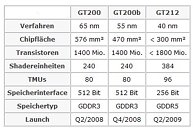
Source:
Hardware-Infos
The transition to GDDR5 seemed inevitable, with there being a genuine incentive of cutting down the number of memory chips (due to the efficient memory bus), with NVIDIA having completely avoided GDDR4. With the die-size being expected to be around 300 sq. mm, these GPUs will be cheaper to manufacture. The GT212 is slated for Q2 2009.

27 Comments on More GT212 Information Forthcoming