
2
Cores
2
Threads
65 W
TDP
3.4 GHz
Frequency
3.6 GHz
Boost
Trinity
Codename
Socket FM2
Socket

Front

Connectivity
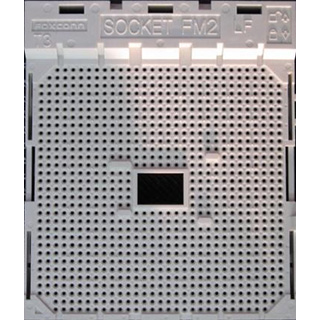
AMD Socket FM2
The AMD A4-5300 was a desktop processor with 2 cores, launched in October 2012. It is part of the A4 lineup, using the Trinity architecture with Socket FM2. A4-5300 has 1 MB of L2 cache and operates at 3.4 GHz by default, but can boost up to 3.6 GHz, depending on the workload. AMD is building the A4-5300 on a 32 nm production process using 1,303 million transistors. The silicon die of the chip is not fabricated at AMD, but at the foundry of GlobalFoundries. The multiplier is locked on A4-5300, which limits its overclocking capabilities.
With a TDP of 65 W, the A4-5300 consumes typical power levels for a modern PC. AMD's processor supports DDR3 memory with a dual-channel interface. For communication with other components in the computer, A4-5300 uses a PCI-Express Gen 2 connection. This processor features the Radeon HD 7480D integrated graphics solution.
Hardware virtualization is available on the A4-5300, which greatly improves virtual machine performance. Programs using Advanced Vector Extensions (AVX) will run on this processor, boosting performance for calculation-heavy applications.
Physical
| Socket: | AMD Socket FM2 |
|---|---|
| Foundry: | GlobalFoundries |
| Process Size: | 32 nm |
| Transistors: | 1,303 million |
| Die Size: | 246 mm² |
| Package: | µPGA |
| tCaseMax: | 70°C |
Processor
| Market: | Desktop |
|---|---|
| Production Status: | End-of-life |
| Release Date: | Oct 2nd, 2012 |
| Part#: | AD5300OKA23HJ AD5300OKHJBOX |
Performance
| Frequency: | 3.4 GHz |
|---|---|
| Turbo Clock: | up to 3.6 GHz |
| Base Clock: | 100 MHz |
| Multiplier: | 36.0x |
| Multiplier Unlocked: | No |
| Voltage: | 1.475 V |
| TDP: | 65 W |
Architecture
| Codename: | Trinity |
|---|---|
| Generation: |
A4
(Trinity) |
| Memory Support: | DDR3 |
| Memory Bus: | Dual-channel |
| ECC Memory: | No |
| PCI-Express: | Gen 2 |
| Chipsets: | A88X, A85X, A78, A75, A68H, A55 |
Core Config
| # of Cores: | 2 |
|---|---|
| # of Threads: | 2 |
| SMP # CPUs: | 1 |
| Integrated Graphics: | Radeon HD 7480D |
Cache
| Cache L1: | 96 KB |
|---|---|
| Cache L2: | 1 MB (shared) |
Features
|
Notes
| 16KB L1 data cache per core. 64KB L1 instruction cache shared per two cores (per module). 1MB L2 cache shared per two cores (per module). 723MHz integrated graphics maximum core frequency. |
May 16th, 2024 09:56 EDT
change timezone
Latest GPU Drivers
New Forum Posts
- AMD RX 7000 series GPU Owners' Club (1108)
- The Official Thermal Interface Material thread (1192)
- What's your latest tech purchase? (20535)
- NVcleanstall error (4)
- 20 Years? (19)
- AIO Water Cooler vs Tower Air Cooler (27)
- Having to login and enable push note every day. (6)
- MSI Z370 SLI PLUS + i9 9900k bad perfomance. (6)
- Ads in forums. under news (12)
- Head Strap & Battery Discussion (0)
Popular Reviews
- Homeworld 3 Performance Benchmark Review - 35 GPUs Tested
- Enermax REVOLUTION D.F. X 1200 W Review
- Lofree Edge Ultra-Low Profile Wireless Mechanical Keyboard Review
- Upcoming Hardware Launches 2023 (Updated Feb 2024)
- ZMF Caldera Closed Planar Magnetic Headphones Review
- AMD Ryzen 7 7800X3D Review - The Best Gaming CPU
- Corsair MP700 Pro SE 4 TB Review
- ASUS Radeon RX 7900 GRE TUF OC Review
- ThundeRobot ML903 NearLink Review
- Sapphire Radeon RX 7900 GRE Pulse Review
Controversial News Posts
- Intel Statement on Stability Issues: "Motherboard Makers to Blame" (267)
- AMD to Redesign Ray Tracing Hardware on RDNA 4 (227)
- Windows 11 Now Officially Adware as Microsoft Embeds Ads in the Start Menu (172)
- NVIDIA to Only Launch the Flagship GeForce RTX 5090 in 2024, Rest of the Series in 2025 (152)
- AMD Hits Highest-Ever x86 CPU Market Share in Q1 2024 Across Desktop and Server (137)
- AMD RDNA 5 a "Clean Sheet" Graphics Architecture, RDNA 4 Merely Corrects a Bug Over RDNA 3 (128)
- AMD's RDNA 4 GPUs Could Stick with 18 Gbps GDDR6 Memory (114)
- AMD Ryzen 9 7900X3D Now at a Mouth-watering $329 (104)