
2
Cores
2
Threads
35 W
TDP
1800 MHz
Frequency
N/A
Boost
Merom
Codename
Socket P
Socket

Front
Intel Socket P
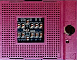
The Intel Core 2 Duo T7100 was a mobile processor with 2 cores, launched in May 2007. It is part of the Core 2 Duo lineup, using the Merom architecture with Socket P. Core 2 Duo T7100 has 2 MB of L2 cache and operates at 1800 MHz. Intel is building the Core 2 Duo T7100 on a 65 nm production process using 293 million transistors. The multiplier is locked on Core 2 Duo T7100, which limits its overclocking capabilities.
With a TDP of 35 W, the Core 2 Duo T7100 consumes only little energy.
The SSE4 instruction set is not supported, which can cause problems with modern games, as they require that capability. Hardware virtualization is available on the Core 2 Duo T7100, which greatly improves virtual machine performance.
Physical
| Socket: | Intel Socket P |
|---|---|
| Foundry: | Intel |
| Process Size: | 65 nm |
| Transistors: | 293 million |
| Die Size: | 111 mm² |
| Package: | FC-PGA |
Processor
| Market: | Mobile |
|---|---|
| Production Status: | End-of-life |
| Release Date: | May 27th, 2007 |
| Part#: | SLA4A |
Performance
| Frequency: | 1800 MHz |
|---|---|
| Turbo Clock: | N/A |
| Base Clock: | 200 MHz |
| Multiplier: | 9.0x |
| Multiplier Unlocked: | No |
| Voltage: | 1.175 V |
| TDP: | 35 W |
Architecture
| Codename: | Merom |
|---|---|
| Generation: |
Core 2 Duo
(Merom) |
| Memory Support: | unknown |
| ECC Memory: | No |
Core Config
| # of Cores: | 2 |
|---|---|
| # of Threads: | 2 |
| SMP # CPUs: | 1 |
| Integrated Graphics: | On certain motherboards (Chipset feature) |
Cache
| Cache L1: | 64 KB |
|---|---|
| Cache L2: | 2 MB |
Features
|
May 21st, 2024 09:24 EDT
change timezone
Latest GPU Drivers
New Forum Posts
- Ryzen 5 5600x stock overclocked reaching high temps (14)
- What are you playing? (20723)
- Gigabyte am5 motherboard ddr5 not posting when rebooting (0)
- Battery swap for cyberpower UPS (92)
- What's your latest tech purchase? (20607)
- My anti budget PC (60)
- MSI RX 580 Armor 8GB VBios (3)
- LG OLED C1 TV odd behaviour after nearly 2 years (57)
- Dell 5400 TPL Help (6)
- Does a faster NVMe make any difference? (18)
Popular Reviews
- Ghost of Tsushima Performance Benchmark Review - 35 GPUs Tested
- Ghost of Tsushima: DLSS vs. FSR vs. XeSS Comparison Review
- PNY XLR8 Gaming EPIC-X RGB DDR5-6400 CL32 32 GB Review
- TerraMaster D8 Hybrid Review
- Silverstone Shark Force 120 mm Fan Review
- Homeworld 3 Performance Benchmark Review - 35 GPUs Tested
- Upcoming Hardware Launches 2023 (Updated Feb 2024)
- Lofree Edge Ultra-Low Profile Wireless Mechanical Keyboard Review
- AMD Ryzen 7 7800X3D Review - The Best Gaming CPU
- AMD Ryzen 7 7700 Review - Affordable Zen 4 Powerhouse
Controversial News Posts
- Intel Statement on Stability Issues: "Motherboard Makers to Blame" (269)
- AMD to Redesign Ray Tracing Hardware on RDNA 4 (227)
- Windows 11 Now Officially Adware as Microsoft Embeds Ads in the Start Menu (173)
- NVIDIA to Only Launch the Flagship GeForce RTX 5090 in 2024, Rest of the Series in 2025 (154)
- AMD Hits Highest-Ever x86 CPU Market Share in Q1 2024 Across Desktop and Server (140)
- AMD RDNA 5 a "Clean Sheet" Graphics Architecture, RDNA 4 Merely Corrects a Bug Over RDNA 3 (139)
- AMD's RDNA 4 GPUs Could Stick with 18 Gbps GDDR6 Memory (114)
- AMD Ryzen 9 7900X3D Now at a Mouth-watering $329 (104)