Report an Error


AMD Litho

Litho

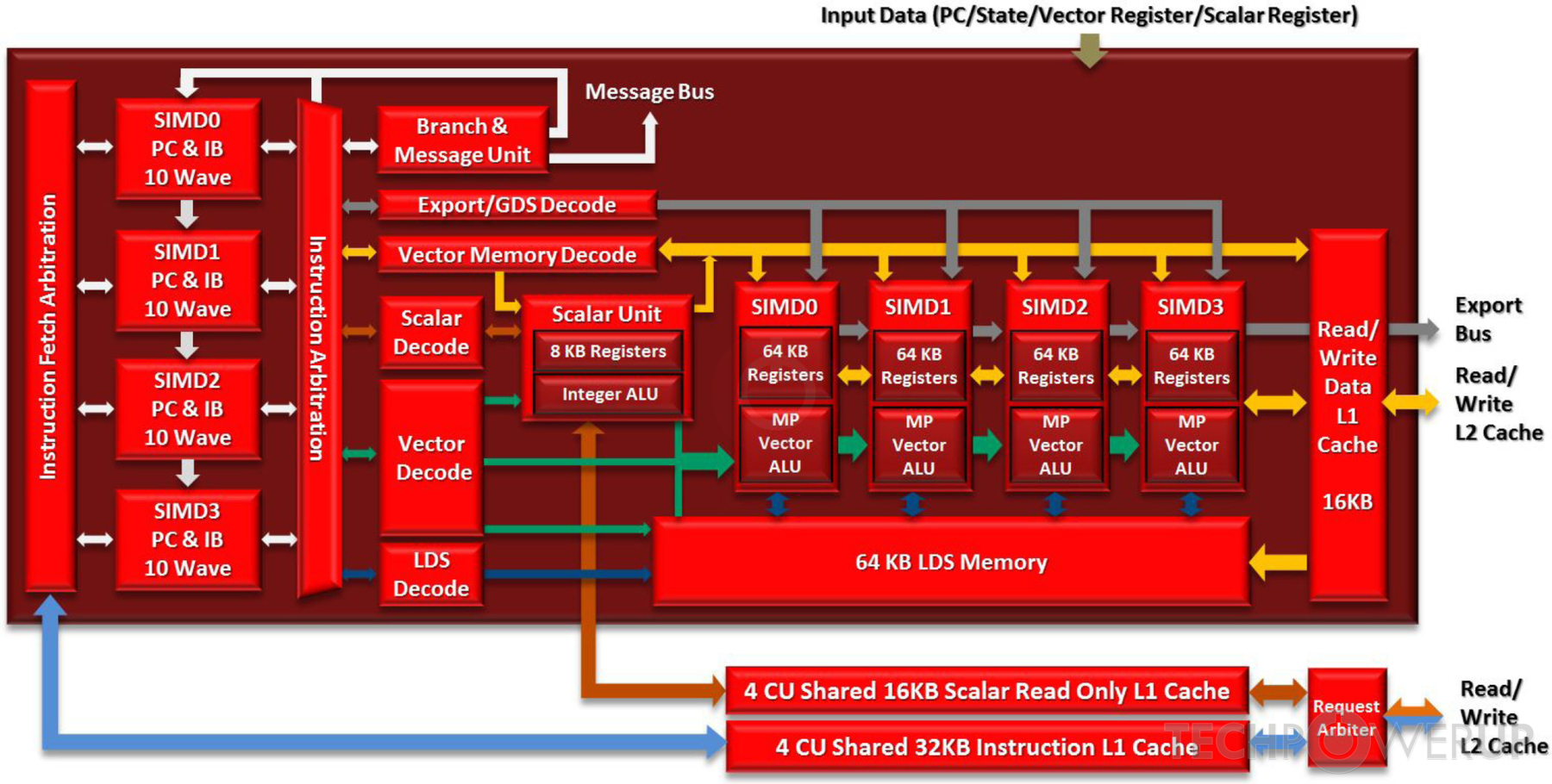
Block Diagram
CU Diagram

LDS Diagram
AMD's Litho GPU uses the GCN 1.0 architecture and is made using a 28 nm production process at TSMC. With a die size of 77 mm² and a transistor count of 950 million it is a very small chip. Litho supports DirectX 12 (Feature Level 11_1). For GPU compute applications, OpenCL version 2.1 (1.2) can be used. It features 384 shading units, 24 texture mapping units and 8 ROPs.
Further reading:
GCN 1.0 Architecture Whitepaper  , Sea Islands Instruction Set Architecture
Graphics Processor
- Released
- May 5th, 2015
- GPU Name
- Litho
- Desktop Variant
- Oland
- Mobile Variant
- Mars / Opal
- Generation
- Sea Islands
- Architecture
- GCN 1.0
- Foundry
- TSMC
- Process Size
- 28 nm
- Transistors
- 950 million
- Density
- 12.3M / mm²
- Die Size
- 77 mm²
- Package
- FCBGA-962
Graphics Features
- DirectX
- 12 (11_1)
- OpenGL
- 4.6
- OpenCL
- 2.1 (1.2)
- Vulkan
- 1.2.170
- Shader Model
- 6.5 (5.1)
- WDDM
- 2.7
- Compute
- GFX6 (gfx601)
- DCE
- 6.4
- UVD
- 4.0
- VCE
- 1.0
- CLRX
- GCN 1.0.0
Render Config
- Shading Units
- 384
- TMUs
- 24
- ROPs
- 8
- Compute Units
- 6
- ACEs
- 2
- GEs
- 1
- L1 Cache
- 16 KB per CU
- L2 Cache
- 256 KB
All GCN 1.0 GPUs
AMD GPU Architecture History
- 2023 CDNA 3.0
- 2022-2024 RDNA 3.0
- 2021 CDNA 2.0
- 2020 CDNA 1.0
- 2020-2023 RDNA 2.0
- 2019-2020 RDNA 1.0
- 2018-2022 GCN 5.1
- 2017-2020 GCN 5.0
- 2016-2020 GCN 4.0
- 2014-2019 GCN 3.0
- 2013-2017 GCN 2.0
- 2011-2020 GCN 1.0
- 2010-2013 TeraScale 3
- 2009-2015 TeraScale 2
- 2005-2013 TeraScale
- 2005-2007 Ultra-Threaded SE
Graphics cards using the AMD Litho GPU
| Name | Chip | Memory | Shaders | TMUs | ROPs | Base Clock | Boost Clock | Memory Clock |
|---|---|---|---|---|---|---|---|---|
| Litho XT | 2 GB | 384 | 24 | 8 | 875 MHz | 960 MHz | 900 MHz | |
| Litho XT | 1024 MB | 384 | 24 | 8 | 825 MHz | 1000 MHz | ||
| Litho XT | 2 GB | 384 | 24 | 8 | 825 MHz | 1000 MHz |
Litho GPU Notes
| Generation: Sea Islands Desktop Variant: Oland Mobile Variant: Mars / Opal Graphics/Compute: GFX6 (gfx601) Display Core Engine: 6.4 Unified Video Decoder: 4.0 Video Compression Engine: 1.0 CLRX: GCN 1.0 |
May 21st, 2024 18:54 EDT
change timezone
Latest GPU Drivers
New Forum Posts
- Gigabyte am5 motherboard ddr5 not posting when rebooting (9)
- Free Games Thread (3818)
- What's your latest tech purchase? (20618)
- Post Your TIMESPY, PCMARK10 & FIRESTRIKE SCORES! (2019) (227)
- For general use - moving files around and playing games, would you have an Optane boot drive or PCie gen 5? (73)
- Can't set PROCHOT offset (0)
- Help to identify component at position U14 on Gigabyte PCB (1)
- CUSTOM RES NOT WORKING AT 144HZ (AMD GPU) (0)
- 3DMARK "LEGENDARY" (193)
- Would you pay more for hardware with AI capabilities? (54)
Popular Reviews
- Ghost of Tsushima Performance Benchmark Review - 35 GPUs Tested
- Ghost of Tsushima: DLSS vs. FSR vs. XeSS Comparison Review
- PNY XLR8 Gaming EPIC-X RGB DDR5-6400 CL32 32 GB Review
- TerraMaster D8 Hybrid Review
- Silverstone Shark Force 120 mm Fan Review
- Homeworld 3 Performance Benchmark Review - 35 GPUs Tested
- Upcoming Hardware Launches 2023 (Updated Feb 2024)
- CHERRY XTRFY M68 Pro Review
- Lofree Edge Ultra-Low Profile Wireless Mechanical Keyboard Review
- AMD Ryzen 7 7800X3D Review - The Best Gaming CPU
Controversial News Posts
- Intel Statement on Stability Issues: "Motherboard Makers to Blame" (269)
- AMD to Redesign Ray Tracing Hardware on RDNA 4 (227)
- Windows 11 Now Officially Adware as Microsoft Embeds Ads in the Start Menu (173)
- NVIDIA to Only Launch the Flagship GeForce RTX 5090 in 2024, Rest of the Series in 2025 (154)
- AMD Hits Highest-Ever x86 CPU Market Share in Q1 2024 Across Desktop and Server (140)
- AMD RDNA 5 a "Clean Sheet" Graphics Architecture, RDNA 4 Merely Corrects a Bug Over RDNA 3 (139)
- AMD's RDNA 4 GPUs Could Stick with 18 Gbps GDDR6 Memory (114)
- AMD Ryzen 9 7900X3D Now at a Mouth-watering $329 (104)