Report an Error


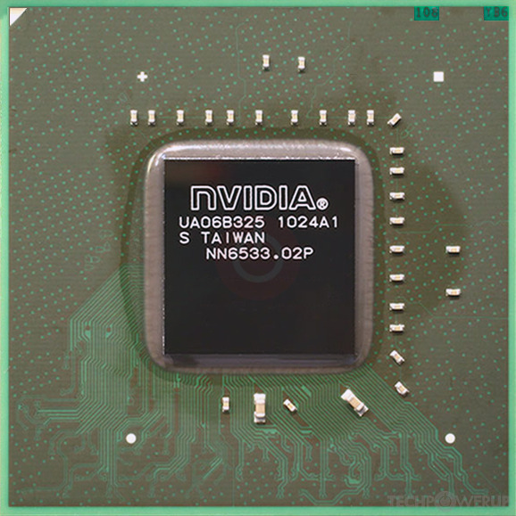
ASUS GT 630M 2 GB
- Graphics Processor
- GF108
- Cores
- 96
- TMUs
- 16
- ROPs
- 4
- Memory Size
- 2 GB
- Memory Type
- DDR3
- Bus Width
- 64 bit
GPU
Graphics Processor
Mobile Graphics
- Release Date
- Mar 22nd, 2012
- Generation
- GeForce 600M
- Predecessor
- GeForce 500M
- Successor
- GeForce 700M
- Production
- End-of-life
- Bus Interface
- MXM-A (3.0)
Clock Speeds
- GPU Clock
475 MHz
672 MHz (+41%)
- Shader Clock
950 MHz
1344 MHz (+41%)
- Memory Clock
-
900 MHz
800 MHz (-11%)
1800 Mbps effective
1600 Mbps effective
Memory
- Memory Size
-
1024 MB
2 GB
- Memory Type
- DDR3
- Memory Bus
- 64 bit
- Bandwidth
-
14.40 GB/s
12.80 GB/s
Render Config
- Shading Units
- 96
- TMUs
- 16
- ROPs
- 4
- SM Count
- 2
- L1 Cache
- 64 KB (per SM)
- L2 Cache
- 128 KB
Theoretical Performance
- Pixel Rate
-
1.900 GPixel/s
2.688 GPixel/s
- Texture Rate
-
7.600 GTexel/s
10.75 GTexel/s
- FP32 (float)
-
182.4 GFLOPS
258.0 GFLOPS
- FP64 (double)
-
15.20 GFLOPS
21.50 GFLOPS (1:12)
Board Design
- Slot Width
- MXM Module
- TDP
- 33 W
- Outputs
- Portable Device Dependent
- Power Connectors
- None
- Board Number
- E1303
Graphics Features
- DirectX
- 12 (11_0)
- OpenGL
- 4.6
- OpenCL
- 1.1
- Vulkan
- N/A
- CUDA
- 2.1
- Shader Model
- 5.1
GF108 GPU Notes
| PureVideo HD: VP4 VDPAU: Feature Set C Latest Drivers: Windows 2000: Quadro Release 261.19 Windows XP / Server 2003 x64: GeForce Release 368.81 Quadro Release R319 U2 (321.01) Windows Vista: GeForce Release 365.19 Quadro Release R346 U7 (348.40) Windows 7 / 8 / 8.1 / 10: GeForce Release 391.35 Quadro Release R375 U11 (377.83) |
Other retail boards based on this design (2)
| Name | GPU Clock | Memory Clock | Other Changes |
|---|---|---|---|
| 672 MHz | 800 MHz | ||
|
ASUS GT 630M 2 GB
|
672 MHz | 800 MHz | 2 GB |
Jun 5th, 2024 02:48 EDT
change timezone
Latest GPU Drivers
New Forum Posts
- Zen5 only 16 core. (52)
- Windows 11 laggy, Intel I7-10610u, Intel UHD graphics 620, asking for advice (1)
- Decent, lightweight alternative to Windows Mail? (25)
- PC Game Retro Reviews (32)
- What's your latest tech purchase? (20735)
- How to check flatness of CPUs and coolers - INK and OPTICAL INTERFERENCE methods (119)
- Insyde software announces AI BIOS! (11)
- Fun times with the NR200P, Dual Rad (no special mods needed) (10)
- All Intel DG1 needs special bios? (28)
- Your PC ATM (34603)
Popular Reviews
- Intel Lunar Lake Technical Deep Dive - So many Revolutions in One Chip
- Kioxia Exceria Plus G3 2 TB Review
- NZXT H6 Flow RGB Review
- Corsair iCUE XC7 RGB Elite LCD CPU Water Block Review
- SilverStone KL07E Review
- Upcoming Hardware Launches 2024 (Updated May 2024)
- NuPhy Air96 V2 Low Profile Wireless Mechanical Keyboard Review
- AMD Ryzen 7 7800X3D Review - The Best Gaming CPU
- Ghost of Tsushima Performance Benchmark Review - 35 GPUs Tested
- ASUS GeForce RTX 4060 Dual OC Review - The Best RTX 4060
Controversial News Posts
- NVIDIA to Only Launch the Flagship GeForce RTX 5090 in 2024, Rest of the Series in 2025 (154)
- AMD Hits Highest-Ever x86 CPU Market Share in Q1 2024 Across Desktop and Server (140)
- AMD RDNA 5 a "Clean Sheet" Graphics Architecture, RDNA 4 Merely Corrects a Bug Over RDNA 3 (139)
- NVIDIA RTX 5090 "Blackwell" Founders Edition to Implement the "RTX 4090 Ti" Cinderblock Design (118)
- Core Configurations of Intel Core Ultra 200 "Arrow Lake-S" Desktop Processors Surface (101)
- Biden Administration to Revive Trump-Era Tariffs on China-made GPUs and Motherboards (95)
- ASRock Innovates First AMD Radeon RX 7000 Graphics Card with 12V-2x6 Power Connector (90)
- AMD Ryzen 9000 Zen 5 Single Thread Performance at 5.80 GHz Found 19% Over Zen 4 (88)