Report an Error


ATI Rage PRO Turbo
Rage PRO Turbo

Rage PRO Turbo A

Rage PRO Turbo P

Fritzchens Fritz
Die Shot
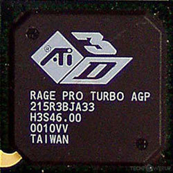
ATI's Rage PRO Turbo GPU uses the Rage 3 architecture and is made using a 350 nm production process at UMC. With a die size of 67 mm² and a transistor count of 8 million it is a very small chip. Rage PRO Turbo supports DirectX 6.0. Modern GPU compute technologies are not available. It features 1 pixel shaders and 0 vertex shaders, 1 texture mapping units and 1 ROPs. Due to the lack of unified shaders you will not be able to run recent games at all (which require unified shader/DX10+ support).
Graphics Processor
- Released
- Mar 1st, 1997
- GPU Name
- Rage PRO Turbo
- Architecture
- Rage 3
- Foundry
- UMC
- Process Size
- 350 nm
- Transistors
- 8 million
- Density
- 119.4K / mm²
- Die Size
- 67 mm²
Graphics Features
- DirectX
- 6.0
- OpenGL
- 1.1
- OpenCL
- N/A
- Vulkan
- N/A
- Pixel Shader
- N/A
- Vertex Shader
- N/A
Render Config
- Pixel Shaders
- 1
- Vertex Shaders
- 0
- TMUs
- 1
- ROPs
- 1
All Rage 3 GPUs
- ATI Rage PRO
- ATI Rage PRO Turbo
- ATI Rage XL
ATI GPU Architecture History
Graphics cards using the ATI Rage PRO Turbo GPU
| Name | Chip | Memory | Shaders | TMUs | ROPs | GPU Clock | Memory Clock |
|---|---|---|---|---|---|---|---|
| Rage PRO Turbo A | 4 MB | 1 / 0 | 1 | 1 | 75 MHz | 75 MHz | |
| Rage PRO Turbo P | 8 MB | 1 / 0 | 1 | 1 | 75 MHz | 75 MHz |


May 3rd, 2024 15:35 EDT
change timezone
Latest GPU Drivers
New Forum Posts
- Announcement: VPN's no longer work right in Windows 10 or 11 or Servers (23)
- Ryzen 7800x3d $196 with bundle at Microcenter (8)
- Alphacool CORE 1 CPU block - bulging with danger of splitting? (75)
- Anime Nation (12783)
- What's your latest tech purchase? (20422)
- DMAS Design [SPDIF-Optical] (76)
- SSD RAM CACHING (Especially Writing) (0)
- 7900 XTX Seriously lacking (113)
- Old high quality PSU, or semi-old mid-quality PSU? (57)
- 7800x3d $216 in bundle at Microcenter (37)
Popular Reviews
- HYTE THICC Q60 240 mm AIO Review
- ASRock NUC BOX-155H (Intel Core Ultra 7 155H) Review
- Meze Audio LIRIC 2nd Generation Closed-Back Headphones Review
- Montech Sky Two GX Review
- Ugreen NASync DXP4800 Plus Review
- Upcoming Hardware Launches 2023 (Updated Feb 2024)
- Team Group T-Force Vulcan ECO DDR5-6000 32 GB CL38 Review
- MOONDROP x Crinacle DUSK In-Ear Monitors Review - The Last 5%
- AMD Ryzen 7 7800X3D Review - The Best Gaming CPU
- Logitech G Pro X Superlight 2 Review - Updated with 4000 Hz Tested
Controversial News Posts
- Intel Statement on Stability Issues: "Motherboard Makers to Blame" (235)
- Windows 11 Now Officially Adware as Microsoft Embeds Ads in the Start Menu (167)
- Sony PlayStation 5 Pro Specifications Confirmed, Console Arrives Before Holidays (117)
- AMD's RDNA 4 GPUs Could Stick with 18 Gbps GDDR6 Memory (114)
- AMD to Redesign Ray Tracing Hardware on RDNA 4 (111)
- NVIDIA Points Intel Raptor Lake CPU Users to Get Help from Intel Amid System Instability Issues (106)
- AMD "Strix Halo" Zen 5 Mobile Processor Pictured: Chiplet-based, Uses 256-bit LPDDR5X (103)
- AMD Ryzen 9 7900X3D Now at a Mouth-watering $329 (103)