Report an Error


NVIDIA CMP 100HX-210
- Graphics Processor
- GV100
- Cores
- 5120
- TMUs
- 320
- ROPs
- 128
- Memory Size
- 16 GB
- Memory Type
- HBM2
- Bus Width
- 4096 bit
GPU
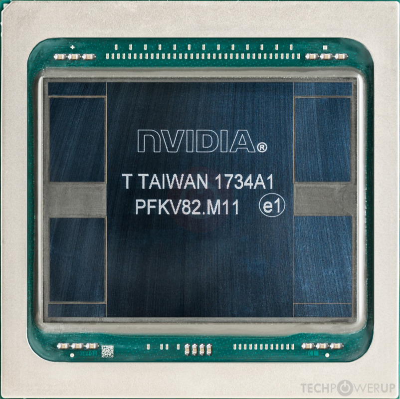
The CMP 100HX-210 was a graphics card by NVIDIA, launched in 2020. Built on the 12 nm process, and based on the GV100 graphics processor, the card supports DirectX 12. This ensures that all modern games will run on CMP 100HX-210. The GV100 graphics processor is a large chip with a die area of 815 mm² and 21,100 million transistors. It features 5120 shading units, 320 texture mapping units, and 128 ROPs. Also included are 640 tensor cores which help improve the speed of machine learning applications. NVIDIA has paired 16 GB HBM2 memory with the CMP 100HX-210, which are connected using a 4096-bit memory interface. The GPU is operating at a frequency of 555 MHz, which can be boosted up to 1147 MHz, memory is running at 810 MHz.
Being a dual-slot card, the NVIDIA CMP 100HX-210 draws power from 1x 6-pin + 1x 8-pin power connector, with power draw rated at 250 W maximum. This device has no display connectivity, as it is not designed to have monitors connected to it. CMP 100HX-210 is connected to the rest of the system using a PCI-Express 3.0 x16 interface. The card's dimensions are 267 mm x 112 mm x 40 mm, and it features a dual-slot cooling solution.
Being a dual-slot card, the NVIDIA CMP 100HX-210 draws power from 1x 6-pin + 1x 8-pin power connector, with power draw rated at 250 W maximum. This device has no display connectivity, as it is not designed to have monitors connected to it. CMP 100HX-210 is connected to the rest of the system using a PCI-Express 3.0 x16 interface. The card's dimensions are 267 mm x 112 mm x 40 mm, and it features a dual-slot cooling solution.
Graphics Processor
Graphics Card
Relative Performance
Based on TPU review data: "Performance Summary" at 1920x1080, 4K for 2080 Ti and faster.
Performance estimated based on architecture, shader count and clocks.
Clock Speeds
- Base Clock
- 555 MHz
- Boost Clock
- 1147 MHz
- Memory Clock
-
810 MHz
1620 Mbps effective
Memory
- Memory Size
- 16 GB
- Memory Type
- HBM2
- Memory Bus
- 4096 bit
- Bandwidth
- 829.4 GB/s
Render Config
- Shading Units
- 5120
- TMUs
- 320
- ROPs
- 128
- SM Count
- 80
- Tensor Cores
- 640
- L1 Cache
- 96 KB (per SM)
- L2 Cache
- 6 MB
Theoretical Performance
- Pixel Rate
- 146.8 GPixel/s
- Texture Rate
- 367.0 GTexel/s
- FP16 (half)
- 23.49 TFLOPS (2:1)
- FP32 (float)
- 11.75 TFLOPS
- FP64 (double)
- 5.873 TFLOPS (1:2)
Board Design
- Slot Width
- Dual-slot
- Length
- 267 mm
10.5 inches
- Width
- 112 mm
4.4 inches
- Height
- 40 mm
1.6 inches
- TDP
- 250 W
- Suggested PSU
- 600 W
- Outputs
- No outputs
- Power Connectors
- 1x 6-pin + 1x 8-pin
- Board Number
- PG500 SKU 0
Graphics Features
- DirectX
- 12 (12_1)
- OpenGL
- 4.6
- OpenCL
- 3.0
- Vulkan
- 1.3
- CUDA
- 7.0
- Shader Model
- 6.7
GV100 GPU Notes
| Tensor Cores: 1st Gen NVENC: 6th Gen NVDEC: 3rd Gen PureVideo HD: VP9 VDPAU: Feature Set I |
Apr 29th, 2024 15:24 EDT
change timezone
Latest GPU Drivers
New Forum Posts
- 7900 XTX Seriously lacking (2)
- i7-1355U (6)
- Show us your collections thread!! (285)
- Is it better for zero RPM PSUs to place the fan on top? (26)
- Z790 ACE MAX? (6)
- What's your latest tech purchase? (20393)
- Dialing in the overlock on my new 12600kf, matured silicon process showing great results... (20)
- Is this Sapphire PULSE RX 5600 XT legit or fake? (16)
- Arctic MX-6 shelf life is just a couple months? (23)
- Throttlestop I7-9750H is there a risk with raising PL1 and PL2? (10)
Popular Reviews
- Ugreen NASync DXP4800 Plus Review
- HYTE THICC Q60 240 mm AIO Review
- Upcoming Hardware Launches 2023 (Updated Feb 2024)
- MOONDROP x Crinacle DUSK In-Ear Monitors Review - The Last 5%
- Thermalright Phantom Spirit 120 EVO Review
- FiiO K19 Desktop DAC/Headphone Amplifier Review
- AMD Ryzen 7 7800X3D Review - The Best Gaming CPU
- ASUS Radeon RX 7900 GRE TUF OC Review
- Logitech G Pro X Superlight 2 Review - Updated with 4000 Hz Tested
- Sapphire Radeon RX 7900 GRE Pulse Review
Controversial News Posts
- Windows 11 Now Officially Adware as Microsoft Embeds Ads in the Start Menu (149)
- Intel Statement on Stability Issues: "Motherboard Makers to Blame" (144)
- Sony PlayStation 5 Pro Specifications Confirmed, Console Arrives Before Holidays (117)
- NVIDIA Points Intel Raptor Lake CPU Users to Get Help from Intel Amid System Instability Issues (106)
- AMD "Strix Halo" Zen 5 Mobile Processor Pictured: Chiplet-based, Uses 256-bit LPDDR5X (103)
- AMD's RDNA 4 GPUs Could Stick with 18 Gbps GDDR6 Memory (102)
- US Government Wants Nuclear Plants to Offload AI Data Center Expansion (98)
- TechPowerUp Hiring: Reviewers Wanted for Motherboards, Laptops, Gaming Handhelds and Prebuilt Desktops (89)