Report an Error
NVIDIA GeForce GT 720 OEM
- Graphics Processor
- GK107
- Cores
- 192
- TMUs
- 16
- ROPs
- 16
- Memory Size
- 1024 MB
- Memory Type
- DDR3
- Bus Width
- 128 bit

GPU
Recommended Gaming Resolutions:
- 1280x720
- 1366x768
- 1600x900
The GeForce GT 720 OEM was a graphics card by NVIDIA, launched on October 29th, 2017. Built on the 28 nm process, and based on the GK107 graphics processor, the card supports DirectX 12. Even though it supports DirectX 12, the feature level is only 11_0, which can be problematic with newer DirectX 12 titles. The GK107 graphics processor is an average sized chip with a die area of 118 mm² and 1,270 million transistors. Unlike the fully unlocked GeForce GT 640 OEM, which uses the same GPU but has all 384 shaders enabled, NVIDIA has disabled some shading units on the GeForce GT 720 OEM to reach the product's target shader count. It features 192 shading units, 16 texture mapping units, and 16 ROPs. NVIDIA has paired 1,024 MB DDR3 memory with the GeForce GT 720 OEM, which are connected using a 128-bit memory interface. The GPU is operating at a frequency of 993 MHz, memory is running at 891 MHz.
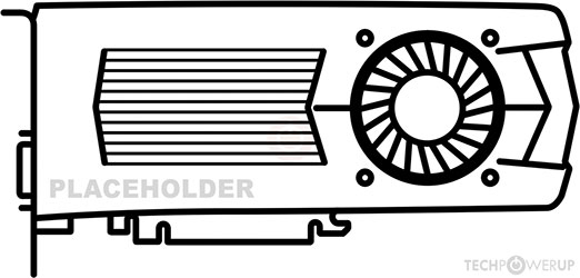
Being a single-slot card, the NVIDIA GeForce GT 720 OEM does not require any additional power connector, its power draw is rated at 50 W maximum. Display outputs include: 1x DVI, 1x HDMI 1.4a, 1x VGA. GeForce GT 720 OEM is connected to the rest of the system using a PCI-Express 3.0 x16 interface. The card measures 145 mm in length, and features a single-slot cooling solution.
Being a single-slot card, the NVIDIA GeForce GT 720 OEM does not require any additional power connector, its power draw is rated at 50 W maximum. Display outputs include: 1x DVI, 1x HDMI 1.4a, 1x VGA. GeForce GT 720 OEM is connected to the rest of the system using a PCI-Express 3.0 x16 interface. The card measures 145 mm in length, and features a single-slot cooling solution.
Graphics Processor
Graphics Card
- Release Date
- Oct 29th, 2017
- Generation
- GeForce 700
- Predecessor
- GeForce 600
- Successor
- GeForce 900
- Production
- End-of-life
- Bus Interface
- PCIe 3.0 x16
Relative Performance
Based on TPU review data: "Performance Summary" at 1920x1080, 4K for 2080 Ti and faster.
Performance estimated based on architecture, shader count and clocks.
Clock Speeds
- GPU Clock
- 993 MHz
- Memory Clock
-
891 MHz
1782 Mbps effective
Memory
- Memory Size
- 1024 MB
- Memory Type
- DDR3
- Memory Bus
- 128 bit
- Bandwidth
- 28.51 GB/s
Render Config
- Shading Units
- 192
- TMUs
- 16
- ROPs
- 16
- SMX Count
- 1
- L1 Cache
- 16 KB (per SMX)
- L2 Cache
- 256 KB
Theoretical Performance
- Pixel Rate
- 3.972 GPixel/s
- Texture Rate
- 15.89 GTexel/s
- FP32 (float)
- 381.3 GFLOPS
- FP64 (double)
- 15.89 GFLOPS (1:24)
Board Design
- Slot Width
- Single-slot
- Length
- 145 mm
5.7 inches
- TDP
- 50 W
- Suggested PSU
- 250 W
- Outputs
- 1x DVI
1x HDMI 1.4a
1x VGA
- Power Connectors
- None
- Board Number
- P2011
Graphics Features
- DirectX
- 12 (11_0)
- OpenGL
- 4.6
- OpenCL
- 3.0
- Vulkan
- 1.2.175
- CUDA
- 3.0
- Shader Model
- 6.5 (5.1)
Card Notes
| some specs unknown |
GK107 GPU Notes
| NVENC: 1st Gen NVDEC: 1st Gen PureVideo HD: VP5 VDPAU: Feature Set D L1 Cache is configurable from 16 KB up to 48 KB per SMX |
May 7th, 2024 19:19 EDT
change timezone
Latest GPU Drivers
New Forum Posts
- Urgent: PC wont turn on with PSU connected to MOBO (7)
- 1GHZ less than I should be getting (6)
- Only some humans can see refresh rates faster than others, I am one of those humans. (215)
- Share your AIDA 64 cache and memory benchmark here (2930)
- not impressed - nvme vs ssd (37)
- What are you playing? (20599)
- XFX RX470 8GB no video and error 43 (33)
- What's your latest tech purchase? (20472)
- Battery swap for cyberpower UPS (63)
- Arkane Austin and Redfall: what happened? (48)
Popular Reviews
- Finalmouse UltralightX Review
- Corsair iCUE Link RX120 RGB 120 mm Fan Review
- CHERRY XTRFY M64 Pro Review
- Cougar Hotrod Royal Gaming Chair Review
- Meze Audio LIRIC 2nd Generation Closed-Back Headphones Review
- Upcoming Hardware Launches 2023 (Updated Feb 2024)
- ASRock NUC BOX-155H (Intel Core Ultra 7 155H) Review
- AMD Ryzen 7 7800X3D Review - The Best Gaming CPU
- ASUS Radeon RX 7900 GRE TUF OC Review
- Logitech G Pro X Superlight 2 Review - Updated with 4000 Hz Tested
Controversial News Posts
- Intel Statement on Stability Issues: "Motherboard Makers to Blame" (254)
- AMD to Redesign Ray Tracing Hardware on RDNA 4 (201)
- Windows 11 Now Officially Adware as Microsoft Embeds Ads in the Start Menu (167)
- NVIDIA to Only Launch the Flagship GeForce RTX 5090 in 2024, Rest of the Series in 2025 (130)
- Sony PlayStation 5 Pro Specifications Confirmed, Console Arrives Before Holidays (119)
- AMD's RDNA 4 GPUs Could Stick with 18 Gbps GDDR6 Memory (114)
- NVIDIA Points Intel Raptor Lake CPU Users to Get Help from Intel Amid System Instability Issues (106)
- AMD Ryzen 9 7900X3D Now at a Mouth-watering $329 (104)