Report an Error


NVIDIA GeForce GTS 250
- Graphics Processor
- G92B
- Cores
- 128
- TMUs
- 64
- ROPs
- 16
- Memory Size
- 1024 MB
- Memory Type
- GDDR3
- Bus Width
- 256 bit

GPU
Recommended Gaming Resolutions:
- 1366x768
- 1600x900
- 1920x1080
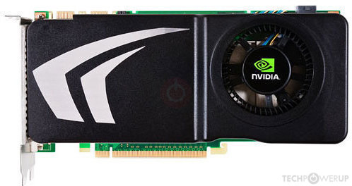
The GeForce GTS 250 was a performance-segment graphics card by NVIDIA, launched on March 4th, 2009. Built on the 55 nm process, and based on the G92B graphics processor, in its G92-426-B1 variant, the card supports DirectX 11.1. Even though it supports DirectX 11, the feature level is only 10_0, which can be problematic with many DirectX 11 & DirectX 12 titles. The G92B graphics processor is an average sized chip with a die area of 260 mm² and 754 million transistors. It features 128 shading units, 64 texture mapping units, and 16 ROPs. NVIDIA has paired 1,024 MB GDDR3 memory with the GeForce GTS 250, which are connected using a 256-bit memory interface. The GPU is operating at a frequency of 675 MHz, memory is running at 1008 MHz.
Being a dual-slot card, the NVIDIA GeForce GTS 250 draws power from 1x 6-pin power connector, with power draw rated at 150 W maximum. Display outputs include: 2x DVI. GeForce GTS 250 is connected to the rest of the system using a PCI-Express 2.0 x16 interface. The card measures 229 mm in length, and features a dual-slot cooling solution. Its price at launch was 199 US Dollars.
Being a dual-slot card, the NVIDIA GeForce GTS 250 draws power from 1x 6-pin power connector, with power draw rated at 150 W maximum. Display outputs include: 2x DVI. GeForce GTS 250 is connected to the rest of the system using a PCI-Express 2.0 x16 interface. The card measures 229 mm in length, and features a dual-slot cooling solution. Its price at launch was 199 US Dollars.
Graphics Processor
Graphics Card
- Release Date
- Mar 4th, 2009
- Generation
- GeForce 200
- Predecessor
- GeForce 9
- Successor
- GeForce 400
- Production
- End-of-life
- Launch Price
- 199 USD
- Bus Interface
- PCIe 2.0 x16
- Reviews
- 58 in our database
Relative Performance
Based on TPU review data: "Performance Summary" at 1920x1080, 4K for 2080 Ti and faster.
Performance estimated based on architecture, shader count and clocks.
Clock Speeds
- GPU Clock
- 675 MHz
- Shader Clock
- 1620 MHz
- Memory Clock
-
1008 MHz
2 Gbps effective
Memory
- Memory Size
- 1024 MB
- Memory Type
- GDDR3
- Memory Bus
- 256 bit
- Bandwidth
- 64.51 GB/s
Render Config
- Shading Units
- 128
- TMUs
- 64
- ROPs
- 16
- SM Count
- 16
- L2 Cache
- 64 KB
Theoretical Performance
- Pixel Rate
- 10.80 GPixel/s
- Texture Rate
- 43.20 GTexel/s
- FP32 (float)
- 414.7 GFLOPS
Board Design
- Slot Width
- Dual-slot
- Length
- 229 mm
9 inches
- TDP
- 150 W
- Suggested PSU
- 450 W
- Outputs
- 2x DVI
- Power Connectors
- 1x 6-pin
- Board Number
- P391 SKU 51,
P391 SKU 52
Graphics Features
- DirectX
- 11.1 (10_0)
- OpenGL
- 3.3
- OpenCL
- 1.1
- Vulkan
- N/A
- CUDA
- 1.1
- Shader Model
- 4.0
Card Notes
| Rebranded 9800 GT |
G92B GPU Notes
| PureVideo HD: VP2 VDPAU: Feature Set A |
Retail boards based on this design (1)
| Name | GPU Clock | Memory Clock | Other Changes |
|---|---|---|---|
| 675 MHz | 1008 MHz | 1x DVI 1x HDMI 1x VGA |

May 21st, 2024 01:18 EDT
change timezone
Latest GPU Drivers
New Forum Posts
- Cooling 7800X3D with Thermalright Phantom Spirit EVO and idle temp is around 60c. Is this normal? (3)
- Apple Vision Pro seems very dissapointing (36)
- What's your latest tech purchase? (20601)
- EK seems to be having major issues (124)
- Intel SSD model codes & SanDisk SSD product codes reference list (4)
- For general use - moving files around and playing games, would you have an Optane boot drive or PCie gen 5? (58)
- Why I love Gaming (6)
- Ice Age 3: Dawn of the Dinosaurs 30 fps problem (4)
- TPU's Nostalgic Hardware Club (18520)
- Kingdom Hearts coming to steam (0)
Popular Reviews
- Ghost of Tsushima Performance Benchmark Review - 35 GPUs Tested
- Ghost of Tsushima: DLSS vs. FSR vs. XeSS Comparison Review
- TerraMaster D8 Hybrid Review
- PNY XLR8 Gaming EPIC-X RGB DDR5-6400 CL32 32 GB Review
- Silverstone Shark Force 120 mm Fan Review
- Homeworld 3 Performance Benchmark Review - 35 GPUs Tested
- Upcoming Hardware Launches 2023 (Updated Feb 2024)
- Lofree Edge Ultra-Low Profile Wireless Mechanical Keyboard Review
- AMD Ryzen 7 7800X3D Review - The Best Gaming CPU
- AMD Ryzen 7 7700 Review - Affordable Zen 4 Powerhouse
Controversial News Posts
- Intel Statement on Stability Issues: "Motherboard Makers to Blame" (269)
- AMD to Redesign Ray Tracing Hardware on RDNA 4 (227)
- Windows 11 Now Officially Adware as Microsoft Embeds Ads in the Start Menu (173)
- NVIDIA to Only Launch the Flagship GeForce RTX 5090 in 2024, Rest of the Series in 2025 (154)
- AMD Hits Highest-Ever x86 CPU Market Share in Q1 2024 Across Desktop and Server (140)
- AMD RDNA 5 a "Clean Sheet" Graphics Architecture, RDNA 4 Merely Corrects a Bug Over RDNA 3 (139)
- AMD's RDNA 4 GPUs Could Stick with 18 Gbps GDDR6 Memory (114)
- AMD Ryzen 9 7900X3D Now at a Mouth-watering $329 (104)