Report an Error


NVIDIA GeForce GTX 1650 Mobile
- Graphics Processor
- TU117
- Cores
- 1024
- TMUs
- 64
- ROPs
- 32
- Memory Size
- 4 GB
- Memory Type
- GDDR6
- Bus Width
- 128 bit
GPU
Recommended Gaming Resolutions:
- 1920x1080
- 2560x1440
- 3840x2160
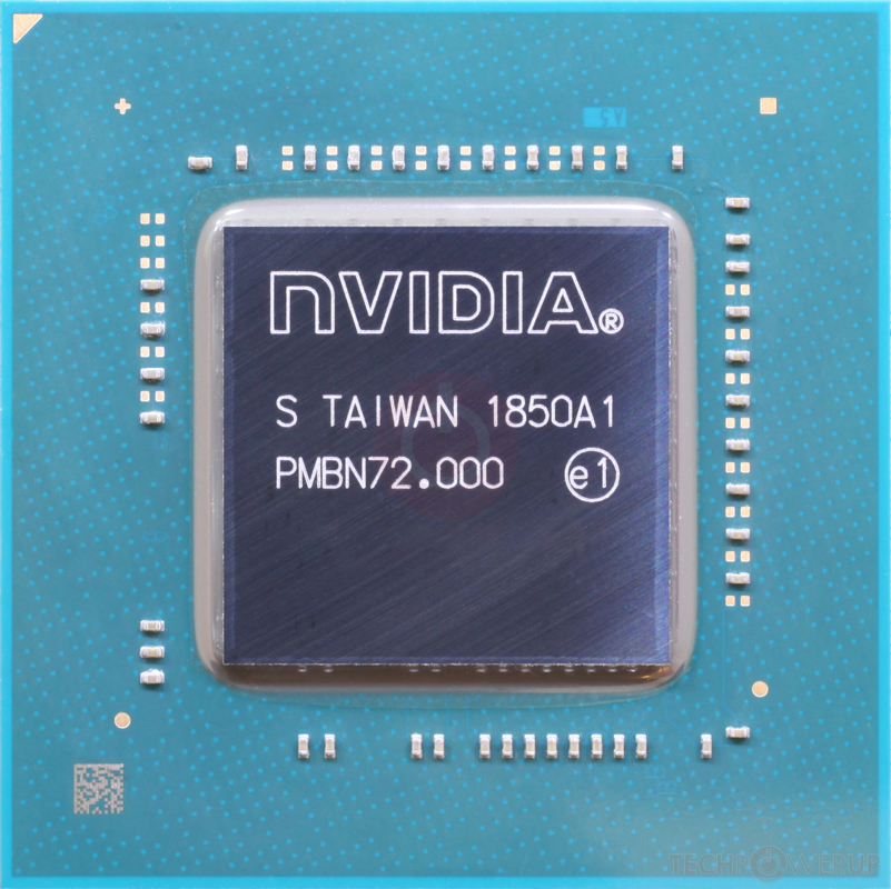
The GeForce GTX 1650 Mobile is a mobile graphics chip by NVIDIA, launched on April 15th, 2020. Built on the 12 nm process, and based on the TU117 graphics processor, in its N18P-G61-MP2 variant, the chip supports DirectX 12. This ensures that all modern games will run on GeForce GTX 1650 Mobile. The TU117 graphics processor is an average sized chip with a die area of 200 mm² and 4,700 million transistors. It features 1024 shading units, 64 texture mapping units, and 32 ROPs. NVIDIA has paired 4 GB GDDR6 memory with the GeForce GTX 1650 Mobile, which are connected using a 128-bit memory interface. The GPU is operating at a frequency of 1380 MHz, which can be boosted up to 1515 MHz, memory is running at 1500 MHz (12 Gbps effective).
Its power draw is rated at 50 W maximum. This device has no display connectivity, as it is not designed to have monitors connected to it. Rather it is intended for use in laptop/notebooks and will use the output of the host mobile device. GeForce GTX 1650 Mobile is connected to the rest of the system using a PCI-Express 3.0 x16 interface.
Its power draw is rated at 50 W maximum. This device has no display connectivity, as it is not designed to have monitors connected to it. Rather it is intended for use in laptop/notebooks and will use the output of the host mobile device. GeForce GTX 1650 Mobile is connected to the rest of the system using a PCI-Express 3.0 x16 interface.
Graphics Processor
Mobile Graphics
- Release Date
- Apr 15th, 2020
- Generation
- GeForce 16 Mobile
- Predecessor
- GeForce 10 Mobile
- Successor
- GeForce 20 Mobile
- Production
- Active
- Bus Interface
- PCIe 3.0 x16
- Reviews
- 45 in our database
Relative Performance
Based on TPU review data: "Performance Summary" at 1920x1080, 4K for 2080 Ti and faster.
Performance estimated based on architecture, shader count and clocks.
Clock Speeds
- Base Clock
- 1380 MHz
- Boost Clock
- 1515 MHz
- Memory Clock
-
1500 MHz
12 Gbps effective
Memory
- Memory Size
- 4 GB
- Memory Type
- GDDR6
- Memory Bus
- 128 bit
- Bandwidth
- 192.0 GB/s
Render Config
- Shading Units
- 1024
- TMUs
- 64
- ROPs
- 32
- SM Count
- 16
- L1 Cache
- 64 KB (per SM)
- L2 Cache
- 1024 KB
Theoretical Performance
- Pixel Rate
- 48.48 GPixel/s
- Texture Rate
- 96.96 GTexel/s
- FP16 (half)
- 6.205 TFLOPS (2:1)
- FP32 (float)
- 3.103 TFLOPS
- FP64 (double)
- 96.96 GFLOPS (1:32)
Board Design
- TDP
- 50 W
- Outputs
- Portable Device Dependent
- Power Connectors
- None
- Board Number
- E4904 SKU 11
Graphics Features
- DirectX
- 12 (12_1)
- OpenGL
- 4.6
- OpenCL
- 3.0
- Vulkan
- 1.3
- CUDA
- 7.5
- Shader Model
- 6.7
TU117 GPU Notes
| NVENC: 5th Gen NVDEC: 4th Gen PureVideo HD: VP10 VDPAU: Feature Set J |
Devices based on this design (3)
| Name | GPU Clock | Boost Clock | Memory Clock | Other Changes |
|---|---|---|---|---|
| 1455 MHz | 1620 MHz | 1500 MHz | ||
| 1455 MHz | 1620 MHz | 1500 MHz | ||
| 1455 MHz | 1620 MHz | 1500 MHz |
May 16th, 2024 07:50 EDT
change timezone
Latest GPU Drivers
New Forum Posts
- Double radiator setup with GPU fans on top (7)
- EULA in Games (18)
- AIO Water Cooler vs Tower Air Cooler (23)
- Would you pay more for hardware with AI capabilities? (21)
- Post Your TIMESPY, PCMARK10 & FIRESTRIKE SCORES! (2019) (220)
- Ads in forums. under news (10)
- Ubuntu 24.04 LTS released (31)
- Homeworld 3 [Official Thread] (42)
- What's your latest tech purchase? (20533)
- Unknown Subvendor in GPU-Z (2)
Popular Reviews
- Homeworld 3 Performance Benchmark Review - 35 GPUs Tested
- Enermax REVOLUTION D.F. X 1200 W Review
- Lofree Edge Ultra-Low Profile Wireless Mechanical Keyboard Review
- Upcoming Hardware Launches 2023 (Updated Feb 2024)
- ZMF Caldera Closed Planar Magnetic Headphones Review
- AMD Ryzen 7 7800X3D Review - The Best Gaming CPU
- Corsair MP700 Pro SE 4 TB Review
- ASUS Radeon RX 7900 GRE TUF OC Review
- ThundeRobot ML903 NearLink Review
- Sapphire Radeon RX 7900 GRE Pulse Review
Controversial News Posts
- Intel Statement on Stability Issues: "Motherboard Makers to Blame" (267)
- AMD to Redesign Ray Tracing Hardware on RDNA 4 (227)
- Windows 11 Now Officially Adware as Microsoft Embeds Ads in the Start Menu (172)
- NVIDIA to Only Launch the Flagship GeForce RTX 5090 in 2024, Rest of the Series in 2025 (152)
- AMD Hits Highest-Ever x86 CPU Market Share in Q1 2024 Across Desktop and Server (137)
- AMD RDNA 5 a "Clean Sheet" Graphics Architecture, RDNA 4 Merely Corrects a Bug Over RDNA 3 (127)
- AMD's RDNA 4 GPUs Could Stick with 18 Gbps GDDR6 Memory (114)
- AMD Ryzen 9 7900X3D Now at a Mouth-watering $329 (104)