Report an Error


NVIDIA GeForce GTX 560 Ti OEM
- Graphics Processor
- GF110
- Cores
- 352
- TMUs
- 44
- ROPs
- 40
- Memory Size
- 1280 MB
- Memory Type
- GDDR5
- Bus Width
- 256 bit

GPU

I/O
Recommended Gaming Resolutions:
- 1600x900
- 1920x1080
- 2560x1440
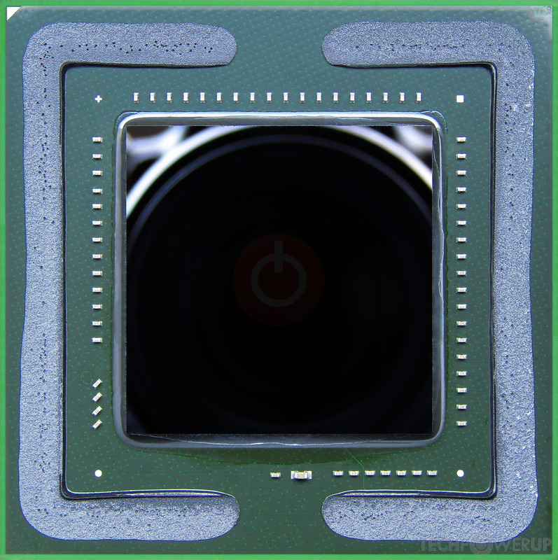
The GeForce GTX 560 Ti OEM was a graphics card by NVIDIA, launched on March 30th, 2011. Built on the 40 nm process, and based on the GF110 graphics processor, the card supports DirectX 12. Even though it supports DirectX 12, the feature level is only 11_0, which can be problematic with newer DirectX 12 titles. The GF110 graphics processor is a large chip with a die area of 520 mm² and 3,000 million transistors. Unlike the fully unlocked GeForce GTX 580, which uses the same GPU but has all 512 shaders enabled, NVIDIA has disabled some shading units on the GeForce GTX 560 Ti OEM to reach the product's target shader count. It features 352 shading units, 44 texture mapping units, and 40 ROPs. NVIDIA has paired 1,280 MB GDDR5 memory with the GeForce GTX 560 Ti OEM, which are connected using a 256-bit memory interface. The GPU is operating at a frequency of 732 MHz, memory is running at 950 MHz (3.8 Gbps effective).
Being a dual-slot card, the NVIDIA GeForce GTX 560 Ti OEM draws power from 2x 6-pin power connectors, with power draw rated at 210 W maximum. Display outputs include: 2x DVI, 1x HDMI 1.3a, 1x DisplayPort. GeForce GTX 560 Ti OEM is connected to the rest of the system using a PCI-Express 2.0 x16 interface. The card measures 229 mm in length, and features a dual-slot cooling solution.
Being a dual-slot card, the NVIDIA GeForce GTX 560 Ti OEM draws power from 2x 6-pin power connectors, with power draw rated at 210 W maximum. Display outputs include: 2x DVI, 1x HDMI 1.3a, 1x DisplayPort. GeForce GTX 560 Ti OEM is connected to the rest of the system using a PCI-Express 2.0 x16 interface. The card measures 229 mm in length, and features a dual-slot cooling solution.
Graphics Processor
Graphics Card
- Release Date
- Mar 30th, 2011
- Generation
- GeForce 500
- Predecessor
- GeForce 400
- Successor
- GeForce 600
- Production
- End-of-life
- Bus Interface
- PCIe 2.0 x16
- Reviews
- 122 in our database
Relative Performance
Based on TPU review data: "Performance Summary" at 1920x1080, 4K for 2080 Ti and faster.
Performance estimated based on architecture, shader count and clocks.
Clock Speeds
- GPU Clock
- 732 MHz
- Shader Clock
- 1464 MHz
- Memory Clock
-
950 MHz
3.8 Gbps effective
Memory
- Memory Size
- 1280 MB
- Memory Type
- GDDR5
- Memory Bus
- 256 bit
- Bandwidth
- 121.6 GB/s
Render Config
- Shading Units
- 352
- TMUs
- 44
- ROPs
- 40
- SM Count
- 11
- L1 Cache
- 64 KB (per SM)
- L2 Cache
- 512 KB
Theoretical Performance
- Pixel Rate
- 16.10 GPixel/s
- Texture Rate
- 32.21 GTexel/s
- FP32 (float)
- 1,031 GFLOPS
- FP64 (double)
- 128.8 GFLOPS (1:8)
Board Design
- Slot Width
- Dual-slot
- Length
- 229 mm
9 inches
- TDP
- 210 W
- Suggested PSU
- 550 W
- Outputs
- 2x DVI
1x HDMI 1.3a
1x DisplayPort
- Power Connectors
- 2x 6-pin
- Board Number
- P1263 SKU 2
Graphics Features
- DirectX
- 12 (11_0)
- OpenGL
- 4.6
- OpenCL
- 1.1
- Vulkan
- N/A
- CUDA
- 2.0
- Shader Model
- 5.1
GF110 GPU Notes
| PureVideo HD: VP4 VDPAU: Feature Set C GF110 has 4 GPCs each capable of 8 pixels per clock. This limits complete GPU to 32 pixels per clock and because of that it can't feed all 48 ROPs when they all require data at the same time. Additional ROPs however can be used for MSAA (because it doesn't require additional data from rasterizers, while giving more work to ROPs.) The complete die contains 64 texture address units and 256 texture filtering units. |
May 1st, 2024 13:31 EDT
change timezone
Latest GPU Drivers
New Forum Posts
- problem with my 7900xtx (20)
- Alphacool CORE 1 CPU block - bulging with danger of splitting? (57)
- TPU's Rosetta Milestones and Daily Pie Thread (1865)
- Recommendation for Android gaming tablet? (2)
- MSI Stealth GS65 9SF settings after repaste (1)
- Old high quality PSU, or semi-old mid-quality PSU? (21)
- Is this Sapphire PULSE RX 5600 XT legit or fake? (23)
- Throttlestop stopped working (VBS is disabled) (1)
- Story saver apps to Instagram (1)
- PC Game Retro Reviews (28)
Popular Reviews
- Ugreen NASync DXP4800 Plus Review
- Team Group T-Force Vulcan ECO DDR5-6000 32 GB CL38 Review
- HYTE THICC Q60 240 mm AIO Review
- Upcoming Hardware Launches 2023 (Updated Feb 2024)
- MOONDROP x Crinacle DUSK In-Ear Monitors Review - The Last 5%
- Montech Sky Two GX Review
- Thermalright Phantom Spirit 120 EVO Review
- AMD Ryzen 7 7800X3D Review - The Best Gaming CPU
- ASUS Radeon RX 7900 GRE TUF OC Review
- FiiO K19 Desktop DAC/Headphone Amplifier Review
Controversial News Posts
- Intel Statement on Stability Issues: "Motherboard Makers to Blame" (210)
- Windows 11 Now Officially Adware as Microsoft Embeds Ads in the Start Menu (157)
- Sony PlayStation 5 Pro Specifications Confirmed, Console Arrives Before Holidays (117)
- AMD's RDNA 4 GPUs Could Stick with 18 Gbps GDDR6 Memory (109)
- NVIDIA Points Intel Raptor Lake CPU Users to Get Help from Intel Amid System Instability Issues (106)
- AMD "Strix Halo" Zen 5 Mobile Processor Pictured: Chiplet-based, Uses 256-bit LPDDR5X (103)
- TechPowerUp Hiring: Reviewers Wanted for Motherboards, Laptops, Gaming Handhelds and Prebuilt Desktops (90)
- Superior Stability by GIGABYTE BETA BIOS with Intel Baseline on Z790/B760 Motherboards (86)