Report an Error


NVIDIA GeForce GTX 950 Low Power
- Graphics Processor
- GM206
- Cores
- 768
- TMUs
- 48
- ROPs
- 32
- Memory Size
- 2 GB
- Memory Type
- GDDR5
- Bus Width
- 128 bit

GPU
Recommended Gaming Resolutions:
- 1600x900
- 1920x1080
- 2560x1440
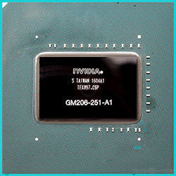
The GeForce GTX 950 Low Power was a mid-range graphics card by NVIDIA, launched on March 1st, 2016. Built on the 28 nm process, and based on the GM206 graphics processor, in its GM206-251-A1 variant, the card supports DirectX 12. This ensures that all modern games will run on GeForce GTX 950 Low Power. The GM206 graphics processor is an average sized chip with a die area of 228 mm² and 2,940 million transistors. Unlike the fully unlocked GeForce GTX 960, which uses the same GPU but has all 1024 shaders enabled, NVIDIA has disabled some shading units on the GeForce GTX 950 Low Power to reach the product's target shader count. It features 768 shading units, 48 texture mapping units, and 32 ROPs. NVIDIA has paired 2,048 MB GDDR5 memory with the GeForce GTX 950 Low Power, which are connected using a 128-bit memory interface. The GPU is operating at a frequency of 1026 MHz, which can be boosted up to 1190 MHz, memory is running at 1653 MHz (6.6 Gbps effective).
Being a dual-slot card, the NVIDIA GeForce GTX 950 Low Power does not require any additional power connector, its power draw is rated at 75 W maximum. Display outputs include: 1x DVI, 1x HDMI 2.0, 3x DisplayPort 1.2. GeForce GTX 950 Low Power is connected to the rest of the system using a PCI-Express 3.0 x16 interface. The card measures 202 mm in length, and features a dual-slot cooling solution. Its price at launch was 159 US Dollars.
Being a dual-slot card, the NVIDIA GeForce GTX 950 Low Power does not require any additional power connector, its power draw is rated at 75 W maximum. Display outputs include: 1x DVI, 1x HDMI 2.0, 3x DisplayPort 1.2. GeForce GTX 950 Low Power is connected to the rest of the system using a PCI-Express 3.0 x16 interface. The card measures 202 mm in length, and features a dual-slot cooling solution. Its price at launch was 159 US Dollars.
Graphics Processor
- GPU Name
- GM206
- GPU Variant
- GM206-251-A1
- Architecture
- Maxwell 2.0
- Foundry
- TSMC
- Process Size
- 28 nm
- Transistors
- 2,940 million
- Density
- 12.9M / mm²
- Die Size
- 228 mm²
- Chip Package
- BGA-1428
Graphics Card
- Release Date
- Mar 1st, 2016
- Generation
- GeForce 900
- Predecessor
- GeForce 700
- Successor
- GeForce 10
- Production
- End-of-life
- Launch Price
- 159 USD
- Bus Interface
- PCIe 3.0 x16
- Reviews
- 76 in our database
Relative Performance
Based on TPU review data: "Performance Summary" at 1920x1080, 4K for 2080 Ti and faster.
Performance estimated based on architecture, shader count and clocks.
Clock Speeds
- Base Clock
- 1026 MHz
- Boost Clock
- 1190 MHz
- Memory Clock
-
1653 MHz
6.6 Gbps effective
Memory
- Memory Size
- 2 GB
- Memory Type
- GDDR5
- Memory Bus
- 128 bit
- Bandwidth
- 105.8 GB/s
Render Config
- Shading Units
- 768
- TMUs
- 48
- ROPs
- 32
- SMM Count
- 6
- L1 Cache
- 48 KB (per SMM)
- L2 Cache
- 1024 KB
Theoretical Performance
- Pixel Rate
- 38.08 GPixel/s
- Texture Rate
- 57.12 GTexel/s
- FP32 (float)
- 1.828 TFLOPS
- FP64 (double)
- 57.12 GFLOPS (1:32)
Board Design
- Slot Width
- Dual-slot
- Length
- 202 mm
8 inches
- TDP
- 75 W
- Suggested PSU
- 250 W
- Outputs
- 1x DVI
1x HDMI 2.0
3x DisplayPort 1.2
- Power Connectors
- None
Graphics Features
- DirectX
- 12 (12_1)
- OpenGL
- 4.6
- OpenCL
- 3.0
- Vulkan
- 1.3
- CUDA
- 5.2
- Shader Model
- 6.7
GM206 GPU Notes
| NVENC: 5th Gen NVDEC: 2nd Gen PureVideo HD: VP7 VDPAU: Feature Set F |
Retail boards based on this design (9)
| Name | GPU Clock | Boost Clock | Memory Clock | Other Changes |
|---|---|---|---|---|
| 1026 MHz | 1190 MHz | 1653 MHz | 211 mm/8.3 inches | |
| 1038 MHz | 1216 MHz | 1653 MHz | ||
| 1026 MHz | 1190 MHz | 1653 MHz | 173 mm/6.8 inches, 1x DVI 1x HDMI 1x DisplayPort | |
| 1026 MHz | 1190 MHz | 1653 MHz | 173 mm/6.8 inches, 2x DVI 1x HDMI 1x DisplayPort | |
| 1127 MHz | 1317 MHz | 1653 MHz | 173 mm/6.8 inches, 2x DVI 1x HDMI 1x DisplayPort | |
| 1127 MHz | 1317 MHz | 1653 MHz | 173 mm/6.8 inches, 1x DVI 1x HDMI 1x DisplayPort | |
| 1038 MHz | 1216 MHz | 1653 MHz | 183 mm/7.2 inches, 1x DVI 1x HDMI 1x DisplayPort | |
| 1076 MHz | 1253 MHz | 1653 MHz | 170 mm/6.7 inches, 1x DVI 1x HDMI 1x DisplayPort | |
| 1038 MHz | 1216 MHz | 1653 MHz | 174 mm/6.9 inches, 1x DVI 1x HDMI 1x DisplayPort |


May 16th, 2024 02:43 EDT
change timezone
Latest GPU Drivers
New Forum Posts
- How to optimize my PC by overclocking my system (17)
- have LGA 1155 motherboard which xeon processor will fit ? (13)
- Double radiator setup with GPU fans on top (2)
- Soundbar or 2.1 speaker for virtual 3d audio in PC games... (20)
- Build From Old Parts (14)
- NVcleanstall error (2)
- Is it normal to hear this sound coming from the psu? (36)
- Ubuntu 24.04 LTS released (27)
- Youtube, Discord, Visual Studio Code are flickering with black checkered squares/vertical lines. Partial solutions to this issue. (401)
- Post your Cinebench 2024 score (461)
Popular Reviews
- Homeworld 3 Performance Benchmark Review - 35 GPUs Tested
- Enermax REVOLUTION D.F. X 1200 W Review
- Upcoming Hardware Launches 2023 (Updated Feb 2024)
- Lofree Edge Ultra-Low Profile Wireless Mechanical Keyboard Review
- ZMF Caldera Closed Planar Magnetic Headphones Review
- AMD Ryzen 7 7800X3D Review - The Best Gaming CPU
- Corsair MP700 Pro SE 4 TB Review
- ASUS Radeon RX 7900 GRE TUF OC Review
- ThundeRobot ML903 NearLink Review
- Sapphire Radeon RX 7900 GRE Pulse Review
Controversial News Posts
- Intel Statement on Stability Issues: "Motherboard Makers to Blame" (267)
- AMD to Redesign Ray Tracing Hardware on RDNA 4 (227)
- Windows 11 Now Officially Adware as Microsoft Embeds Ads in the Start Menu (172)
- NVIDIA to Only Launch the Flagship GeForce RTX 5090 in 2024, Rest of the Series in 2025 (152)
- AMD Hits Highest-Ever x86 CPU Market Share in Q1 2024 Across Desktop and Server (137)
- AMD RDNA 5 a "Clean Sheet" Graphics Architecture, RDNA 4 Merely Corrects a Bug Over RDNA 3 (124)
- AMD's RDNA 4 GPUs Could Stick with 18 Gbps GDDR6 Memory (114)
- AMD Ryzen 9 7900X3D Now at a Mouth-watering $329 (104)