Report an Error


NVIDIA GeForce RTX 2070 SUPER Mobile
- Graphics Processor
- TU104
- Cores
- 2560
- TMUs
- 160
- ROPs
- 64
- Memory Size
- 8 GB
- Memory Type
- GDDR6
- Bus Width
- 256 bit
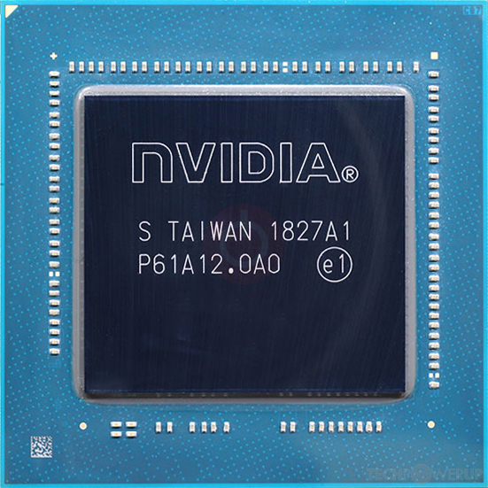
GPU
Recommended Gaming Resolutions:
- 1920x1080
- 2560x1440
- 3840x2160
The GeForce RTX 2070 SUPER Mobile is a mobile graphics chip by NVIDIA, launched on April 2nd, 2020. Built on the 12 nm process, and based on the TU104 graphics processor, in its N18E-G2R variant, the chip supports DirectX 12 Ultimate. This ensures that all modern games will run on GeForce RTX 2070 SUPER Mobile. Additionally, the DirectX 12 Ultimate capability guarantees support for hardware-raytracing, variable-rate shading and more, in upcoming video games. The TU104 graphics processor is a large chip with a die area of 545 mm² and 13,600 million transistors. Unlike the fully unlocked GeForce RTX 2080 SUPER, which uses the same GPU but has all 3072 shaders enabled, NVIDIA has disabled some shading units on the GeForce RTX 2070 SUPER Mobile to reach the product's target shader count. It features 2560 shading units, 160 texture mapping units, and 64 ROPs. Also included are 320 tensor cores which help improve the speed of machine learning applications. The card also has 40 raytracing acceleration cores. NVIDIA has paired 8 GB GDDR6 memory with the GeForce RTX 2070 SUPER Mobile, which are connected using a 256-bit memory interface. The GPU is operating at a frequency of 1140 MHz, which can be boosted up to 1380 MHz, memory is running at 1750 MHz (14 Gbps effective).
Being a mxm module card, the NVIDIA GeForce RTX 2070 SUPER Mobile does not require any additional power connector, its power draw is rated at 115 W maximum. This device has no display connectivity, as it is not designed to have monitors connected to it. Rather it is intended for use in laptop/notebooks and will use the output of the host mobile device. GeForce RTX 2070 SUPER Mobile is connected to the rest of the system using a PCI-Express 3.0 x16 interface.
Being a mxm module card, the NVIDIA GeForce RTX 2070 SUPER Mobile does not require any additional power connector, its power draw is rated at 115 W maximum. This device has no display connectivity, as it is not designed to have monitors connected to it. Rather it is intended for use in laptop/notebooks and will use the output of the host mobile device. GeForce RTX 2070 SUPER Mobile is connected to the rest of the system using a PCI-Express 3.0 x16 interface.
Graphics Processor
Mobile Graphics
- Release Date
- Apr 2nd, 2020
- Generation
- GeForce 20 Mobile
- Predecessor
- GeForce 10 Mobile
- Successor
- GeForce 30 Mobile
- Production
- Active
- Bus Interface
- PCIe 3.0 x16
Relative Performance
Based on TPU review data: "Performance Summary" at 1920x1080, 4K for 2080 Ti and faster.
Performance estimated based on architecture, shader count and clocks.
Clock Speeds
- Base Clock
- 1140 MHz
- Boost Clock
- 1380 MHz
- Memory Clock
-
1750 MHz
14 Gbps effective
Memory
- Memory Size
- 8 GB
- Memory Type
- GDDR6
- Memory Bus
- 256 bit
- Bandwidth
- 448.0 GB/s
Render Config
- Shading Units
- 2560
- TMUs
- 160
- ROPs
- 64
- SM Count
- 40
- Tensor Cores
- 320
- RT Cores
- 40
- L1 Cache
- 64 KB (per SM)
- L2 Cache
- 4 MB
Theoretical Performance
- Pixel Rate
- 88.32 GPixel/s
- Texture Rate
- 220.8 GTexel/s
- FP16 (half)
- 14.13 TFLOPS (2:1)
- FP32 (float)
- 7.066 TFLOPS
- FP64 (double)
- 220.8 GFLOPS (1:32)
Board Design
- Slot Width
- MXM Module
- TDP
- 115 W
- Outputs
- Portable Device Dependent
- Power Connectors
- None
- Board Number
- E4914 SKU 11
Graphics Features
- DirectX
- 12 Ultimate (12_2)
- OpenGL
- 4.6
- OpenCL
- 3.0
- Vulkan
- 1.3
- CUDA
- 7.5
- Shader Model
- 6.7
TU104 GPU Notes
| Ray Tracing Cores: 1st Gen Tensor Cores: 2nd Gen NVENC: 7th Gen NVDEC: 4th Gen PureVideo HD: VP10 VDPAU: Feature Set J |
May 18th, 2024 12:04 EDT
change timezone
Latest GPU Drivers
New Forum Posts
- How Much Storage Is Enough To You? (232)
- is there anyway to verify my motherboard actually has a gen5 gpu slot without a gen5 card? (26)
- What are you playing? (20681)
- What's your latest tech purchase? (20562)
- Safe to replace keycaps with new custom ones? (5)
- Unlocked Realtek HD Audio Drivers for Windows 11 (Dolby Digital Live/DTS Interactive) (160)
- Ryzen Owners Zen Garden (7392)
- I make new budgeout build. Tell me ,where i dont see wrong choices... (4)
- Do you use Linux? (260)
- EK seems to be having major issues (101)
Popular Reviews
- Ghost of Tsushima Performance Benchmark Review - 35 GPUs Tested
- Homeworld 3 Performance Benchmark Review - 35 GPUs Tested
- Lofree Edge Ultra-Low Profile Wireless Mechanical Keyboard Review
- Silverstone Shark Force 120 mm Fan Review
- Enermax REVOLUTION D.F. X 1200 W Review
- Sapphire Radeon RX 7900 GRE Pulse Review
- Upcoming Hardware Launches 2023 (Updated Feb 2024)
- TerraMaster D8 Hybrid Review
- AMD Ryzen 7 7800X3D Review - The Best Gaming CPU
- ZMF Caldera Closed Planar Magnetic Headphones Review
Controversial News Posts
- Intel Statement on Stability Issues: "Motherboard Makers to Blame" (269)
- AMD to Redesign Ray Tracing Hardware on RDNA 4 (227)
- Windows 11 Now Officially Adware as Microsoft Embeds Ads in the Start Menu (172)
- NVIDIA to Only Launch the Flagship GeForce RTX 5090 in 2024, Rest of the Series in 2025 (154)
- AMD Hits Highest-Ever x86 CPU Market Share in Q1 2024 Across Desktop and Server (139)
- AMD RDNA 5 a "Clean Sheet" Graphics Architecture, RDNA 4 Merely Corrects a Bug Over RDNA 3 (130)
- AMD's RDNA 4 GPUs Could Stick with 18 Gbps GDDR6 Memory (114)
- AMD Ryzen 9 7900X3D Now at a Mouth-watering $329 (104)